参数资料
| 型号: | NB4N507ADEVB |
| 厂商: | ON Semiconductor |
| 文件页数: | 1/6页 |
| 文件大小: | 0K |
| 描述: | BOARD EVAL FOR BBG NB4N507AD |
| 标准包装: | 1 |
| 系列: | * |
�� �
�
�NB4N507ADEVB�
�NB4N507ADEVB� Evaluation�
�Board� User's� Manual�
�http://onsemi.com�
�Description�
�The� NB4N507ADEVB� Evaluation� Board� provides� a�
�flexible� and� convenient� platform� to� quickly� evaluate,�
�characterize� and� verify� the� performance� and� operation� of� the�
�NB4N507A� PECL� Clock� Synthesizer.� This� user� ’s� manual�
�provides� detailed� information� on� board� contents,� layout� and�
�its� use.� It� should� be� used� in� conjunction� with� a� device�
�datasheet:� NB4N507A.� (www.onsemi.com)�
�Board� Features�
�?� Accommodates� the� Electrical� Characterization� of� the�
�NB4N507A� in� 16� ?� pin� 150� mil� SOIC� Package�
�?� Supports� use� of� a� 10� MHz� to� 27� MHz� Through� ?� hole� or�
�Surface� Mount� Crystal�
�?� Incorporates� on� Board� Slide� Switch� Controlled�
�Multiplier� Select� and� OE� Logic� Pins,� Minimizing�
�Excess� Cabling�
�?� SMA� Connectors� are� Provided� for� Auxiliary� Input� and�
�Output� Interfaces�
�?� Differential� PECL� Outputs� Loaded/Terminated�
�On� ?� board;� Output� Signals� are� Monitored� via� SMA�
�Connectors�
�?� Convenient� and� Compact� Board� Layout�
�?� 3.3� V� or� 5.0� V� Single� or� Split� ?� Power� Supply� Operation�
�EVAL� BOARD� USER’S� MANUAL�
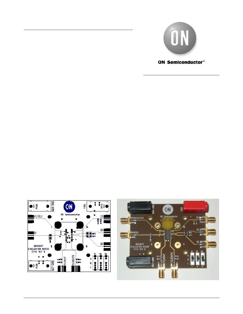
�Board� Layout�
�The� evaluation� board� is� constructed� with� Getek� material�
�with� 50� W� trace� impedances� and� is� designed� to� minimize�
�noise,� achieve� high� bandwidth� and� minimize� crosstalk.�
�The� NB4N507A� evaluation� board� is� equipped� with�
�3� ?� position� slide� switches.� These� switches� are� used� to�
�manipulate� the� static� input� logic� levels� of� the� Multiplier�
�Select� pins,� S0� and� S1,� and� Output� Enable� pin,� OE.� The� H�
�position� of� the� slide� switch� asserts� a� logic� HIGH� on� the�
�assigned� pin,� the� L� asserts� a� logic� LOW� and� the� M� is� an� open�
�where� the� pin� “floats”� to� a� mid� ?� logic� level� by� way� of� the�
�device’s� internal� pull� ?� up� and� pulldown� resistors.�
�Multiplier� Select� pins,� S0� and� S1,� and� Output� Enable� pin,�
�OE,� also� have� SMA� connector� provisions,� if� the� application�
�requires� them.�
�Layer� Stack�
�L1� Signal�
�L2� SMA� Ground�
�L3� V� CC� (Positive� Power� Supply)� and� DUTGND�
�(Device� Ground,� Negative� Power� Supply)�
�L4� Signal�
�Figure� 1.� Evaluation� Board�
�?� Semiconductor� Components� Industries,� LLC,� 2012�
�April,� 2012� ?� Rev.� 2�
�1�
�Publication� Order� Number:�
�EVBUM2074/D�
�相关PDF资料 |
PDF描述 |
|---|---|
| NB4N855SMEVB | CUSTOMER EVALUATION BRD |
| NB6L11MMNGEVB | BOARD EVAL NB6L11MMN CLK BUFFER |
| NB6L239MNEVB | BOARD EVAL BBG NB6L239MND |
| NB7L32MMNEVB | BOARD EVAL FOR NB7L32MM |
| NB7N017MEVB | BOARD EVAL BBG NB7N017MMN |
相关代理商/技术参数 |
参数描述 |
|---|---|
| NB4N507ADG | 功能描述:锁相环 - PLL 3.3V/5V PECL Clock Synthesizer RoHS:否 制造商:Silicon Labs 类型:PLL Clock Multiplier 电路数量:1 最大输入频率:710 MHz 最小输入频率:0.002 MHz 输出频率范围:0.002 MHz to 808 MHz 电源电压-最大:3.63 V 电源电压-最小:1.71 V 最大工作温度:+ 85 C 最小工作温度:- 40 C 封装 / 箱体:QFN-36 封装:Tray |
| NB4N507ADR2 | 功能描述:锁相环 - PLL 3.3V/5V PECL Clock RoHS:否 制造商:Silicon Labs 类型:PLL Clock Multiplier 电路数量:1 最大输入频率:710 MHz 最小输入频率:0.002 MHz 输出频率范围:0.002 MHz to 808 MHz 电源电压-最大:3.63 V 电源电压-最小:1.71 V 最大工作温度:+ 85 C 最小工作温度:- 40 C 封装 / 箱体:QFN-36 封装:Tray |
| NB4N507ADR2G | 功能描述:锁相环 - PLL 3.3V/5V PECL Clock Synthesizer RoHS:否 制造商:Silicon Labs 类型:PLL Clock Multiplier 电路数量:1 最大输入频率:710 MHz 最小输入频率:0.002 MHz 输出频率范围:0.002 MHz to 808 MHz 电源电压-最大:3.63 V 电源电压-最小:1.71 V 最大工作温度:+ 85 C 最小工作温度:- 40 C 封装 / 箱体:QFN-36 封装:Tray |
| NB4N527S | 制造商:ONSEMI 制造商全称:ON Semiconductor 功能描述:3.3V, 2.5Gb/s Dual AnyLevel⑩ to LVDS Receiver/Driver/Buffer/Translator with Internal Input Termination |
| NB4N527SMN | 功能描述:时钟驱动器及分配 3.3V 2.5Gb/s Dual RoHS:否 制造商:Micrel 乘法/除法因子:1:4 输出类型:Differential 最大输出频率:4.2 GHz 电源电压-最大: 电源电压-最小:5 V 最大工作温度:+ 85 C 封装 / 箱体:SOIC-8 封装:Reel |
发布紧急采购,3分钟左右您将得到回复。