参数资料
| 型号: | NB6L11MMNGEVB |
| 厂商: | ON Semiconductor |
| 文件页数: | 1/9页 |
| 文件大小: | 0K |
| 描述: | BOARD EVAL NB6L11MMN CLK BUFFER |
| 标准包装: | 1 |
| 主要目的: | 计时,时钟分配 |
| 嵌入式: | 否 |
| 已用 IC / 零件: | NB6L11M |
| 已供物品: | 板 |
| 其它名称: | NB6L11MMNGEVB-ND NB6L11MMNGEVBOS |
�� �
�
�NB6L11M�
�2.5V� /� 3.3V� 1:2� Differential�
�CML� Fanout� Buffer�
�Multi� ?� Level� Inputs� w/� Internal� Termination�
�NB6L�
�11M�
�ALYW� G�
�G�
�Q0�
�Q1�
�Q1�
�Description�
�The� NB6L11M� is� a� differential� 1:2� CML� fanout� buffer.� The�
�differential� inputs� incorporate� internal� 50� W� termination� resistors� that�
�are� accessed� through� the� V� T� pins� and� will� accept� LVPECL,� LVCMOS,�
�LVTTL,� CML,� or� LVDS� logic� levels.�
�The� V� REFAC� pin� is� an� internally� generated� voltage� supply� available�
�to� this� device� only.� V� REFAC� is� used� as� a� reference� voltage� for�
�single� ?� ended� PECL� or� NECL� inputs.� For� all� single� ?� ended� input�
�conditions,� the� unused� complementary� differential� input� is� connected�
�to� V� REFAC� as� a� switching� reference� voltage.� V� REFAC� may� also� rebias�
�capacitor� ?� coupled� inputs.� When� used,� decouple� V� REFAC� with� a�
�0.01� m� F� capacitor� and� limit� current� sourcing� or� sinking� to� 0.5� mA.�
�When� not� used,� V� REFAC� output� should� be� left� open.�
�The� device� is� housed� in� a� small� 3x3� mm� 16� pin� QFN� package.�
�The� NB6L11M� is� a� member� of� the� ECLinPS� MAX� t� family� of�
�high� performance� clock� products.�
�Features�
�?� Maximum� Input� Clock� Frequency� >� 4� GHz,� Typical�
�?� 225� ps� Typical� Propagation� Delay�
�?� 70� ps� Typical� Rise� and� Fall� Times�
�?� 0.5� ps� maximum� RMS� Clock� Jitter�
�?� Differential� CML� Outputs,� 380� mV� peak� ?� to� ?� peak,� typical�
�?� LVPECL� Operating� Range:� V� CC� =� 2.375� V� to� 3.63� V� with� V� EE� =� 0� V�
�?� NECL� Operating� Range:� V� CC� =� 0� V� with� V� EE� =� ?� 2.375� V� to� ?� 3.63� V�
�?� Internal� Input� Termination� Resistors,� 50� W�
�?� VREFAC� Reference� Output�
�?� Functionally� Compatible� with� Existing� 2.5� V� /� 3.3V� LVEL,� LVEP,�
�EP,� and� SG� Devices�
�?� ?� 40� °� C� to� +85� °� C� Ambient� Operating� Temperature�
�?� These� are� Pb� ?� Free� Devices�
�http://onsemi.com�
�MARKING�
�DIAGRAM*�
�16�
�1�
�QFN� ?� 16�
�MN� SUFFIX�
�CASE� 485G�
�A� =� Assembly� Location�
�L� =� Wafer� Lot�
�Y� =� Year�
�W� =� Work� Week�
�G� =� Pb� ?� Free� Package�
�(Note:� Microdot� may� be� in� either� location)�
�*For� additional� marking� information,� refer� to�
�Application� Note� AND8002/D.�
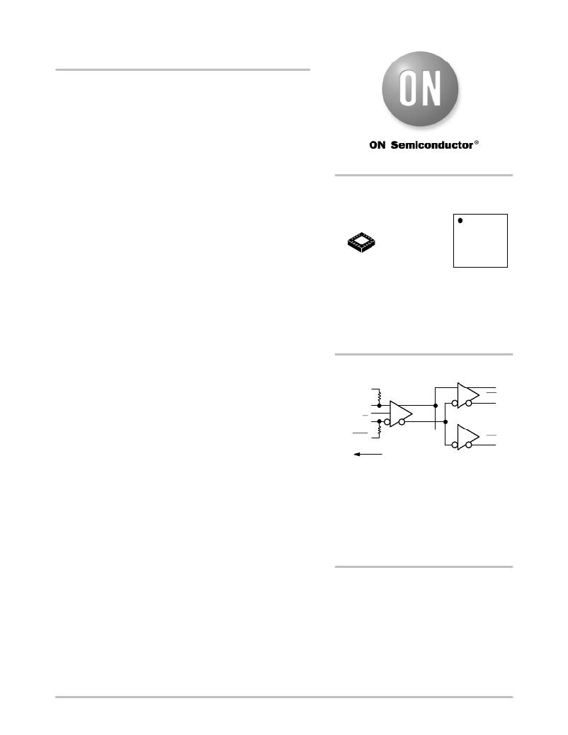
�Q0�
�VTD�
�D�
�D�
�VTD�
�V� REFAC�
�Figure� 1.� Simplified� Logic� Diagram�
�ORDERING� INFORMATION�
�See� detailed� ordering� and� shipping� information� in� the� package�
�dimensions� section� on� page� 8� of� this� data� sheet.�
�?� Semiconductor� Components� Industries,� LLC,� 2009�
�August,� 2009� ?� Rev.� 4�
�1�
�Publication� Order� Number:�
�NB6L11M/D�
�相关PDF资料 |
PDF描述 |
|---|---|
| NB6L239MNEVB | BOARD EVAL BBG NB6L239MND |
| NB7L32MMNEVB | BOARD EVAL FOR NB7L32MM |
| NB7N017MEVB | BOARD EVAL BBG NB7N017MMN |
| NC2003SR | STAND NOTEBOOK W/2FANS USB |
| NCN9252MUGEVB | BOARD EVALUATION NCN9252MU |
相关代理商/技术参数 |
参数描述 |
|---|---|
| NB6L11MMNR2G | 功能描述:时钟缓冲器 1:2 CML FANOUT RoHS:否 制造商:Texas Instruments 输出端数量:5 最大输入频率:40 MHz 传播延迟(最大值): 电源电压-最大:3.45 V 电源电压-最小:2.375 V 最大功率耗散: 最大工作温度:+ 85 C 最小工作温度:- 40 C 封装 / 箱体:LLP-24 封装:Reel |
| NB6L11S | 制造商:ONSEMI 制造商全称:ON Semiconductor 功能描述:2.5 V 1:2 AnyLevel TM Input to LVDS Fanout Buffer / Translator |
| NB6L11S_06 | 制造商:ONSEMI 制造商全称:ON Semiconductor 功能描述:2.5 V 1:2 AnyLevel TM Input to LVDS Fanout Buffer / Translator |
| NB6L11SMNG | 功能描述:时钟缓冲器 HF LVDS FANOUT BUFF/ TRANS RoHS:否 制造商:Texas Instruments 输出端数量:5 最大输入频率:40 MHz 传播延迟(最大值): 电源电压-最大:3.45 V 电源电压-最小:2.375 V 最大功率耗散: 最大工作温度:+ 85 C 最小工作温度:- 40 C 封装 / 箱体:LLP-24 封装:Reel |
| NB6L11SMNGEVB | 功能描述:BOARD EVAL FOR NB6L11SMNG RoHS:是 类别:编程器,开发系统 >> 评估演示板和套件 系列:- 标准包装:1 系列:PCI Express® (PCIe) 主要目的:接口,收发器,PCI Express 嵌入式:- 已用 IC / 零件:DS80PCI800 主要属性:- 次要属性:- 已供物品:板 |
发布紧急采购,3分钟左右您将得到回复。