参数资料
| 型号: | NB6L11MMNGEVB |
| 厂商: | ON Semiconductor |
| 文件页数: | 2/9页 |
| 文件大小: | 0K |
| 描述: | BOARD EVAL NB6L11MMN CLK BUFFER |
| 标准包装: | 1 |
| 主要目的: | 计时,时钟分配 |
| 嵌入式: | 否 |
| 已用 IC / 零件: | NB6L11M |
| 已供物品: | 板 |
| 其它名称: | NB6L11MMNGEVB-ND NB6L11MMNGEVBOS |
�� �
�
�NB6L11M�
�V� CC�
�V� EE� V� EE�
�V� C� C�
�Exposed� Pad� (EP)�
�16�
�15�
�14�
�13�
�VTD�
�D�
�1�
�2�
�12�
�11�
�Q0�
�Q0�
�NB6L11M�
�D�
�VTD�
�3�
�4�
�10�
�9�
�Q1�
�Q1�
�5�
�6�
�7�
�8�
�V� CC� V� REFAC� V� EE�
�V� CC�
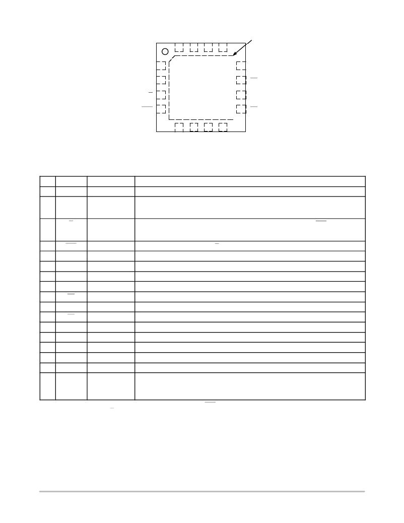
�Figure� 2.� Pin� Configuration� (Top� View)�
�Table� 1.� PIN� DESCRIPTION�
�Pin�
�1�
�2�
�3�
�4�
�5�
�6�
�7�
�8�
�9�
�10�
�11�
�12�
�13�
�14�
�15�
�16�
�?�
�Name�
�VTD�
�D�
�D�
�VTD�
�V� CC�
�V� REFAC�
�V� EE�
�V� CC�
�Q1�
�Q1�
�Q0�
�Q0�
�V� CC�
�V� EE�
�V� EE�
�V� CC�
�EP�
�I/O�
�?�
�ECL,� CML,�
�LVCMOS,� LVDS,�
�LVTTL� Input�
�ECL,� CML,�
�LVCMOS,� LVDS,�
�LVTTL� Input�
�?�
�?�
�?�
�?�
�CML� Output�
�CML� Output�
�CML� Output�
�CML� Output�
�?�
�?�
�?�
�?�
�?�
�Description�
�Internal� 50� W� Termination� Pin� for� D� input.�
�Noninverted� Differential� Input.� Note� 1.� Internal� 50� W� Resistor� to� Termination� Pin,� VTD.�
�Inverted� Differential� Input.� Note� 1.� Internal� 50� W� Resistor� to� Termination� Pin,� VTD.�
�Internal� 50� W� Termination� Pin� for� D� input.�
�Positive� Supply� Voltage�
�Output� Reference� Voltage� for� direct� or� capacitor� coupled� inputs�
�Negative� Supply� Voltage�
�Positive� Supply� Voltage�
�Inverted� Differential� Output.� Typically� Terminated� with� 50� W� Resistor� to� V� CC� .�
�Noninverted� Differential� Output.� Typically� Terminated� with� 50� W� Resistor� to� V� CC� .�
�Inverted� Differential� Output.� Typically� Terminated� with� 50� W� Resistor� to� V� CC� .�
�Noninverted� Differential� Output.� Typically� Terminated� with� 50� W� Resistor� to� V� CC� .�
�Positive� Supply� Voltage�
�Negative� Supply� Voltage�
�Negative� Supply� Voltage�
�Positive� Supply� Voltage�
�The� Exposed� Pad� (EP)� on� the� QFN� ?� 16� package� bottom� is� thermally� connected� to� the� die� for�
�improved� heat� transfer� out� of� package.� The� exposed� pad� must� be� attached� to� a� heat� ?� sinking�
�conduit.� The� pad� is� not� electrically� connected� to� the� die,� but� is� recommended� to� be� electrically�
�and� thermally� connected� to� VEE� on� the� PC� board.�
�1.� In� the� differential� configuration� when� the� input� termination� pins� (VTD,� VTD)� are� connected� to� a� common� termination� voltage� or� left� open,� and�
�if� no� signal� is� applied� on� D/D� input,� then,� the� device� will� be� susceptible� to� self� ?� oscillation.�
�2.� All� V� CC� and� V� EE� pins� must� be� externally� connected� to� a� power� supply� for� proper� operation.�
�http://onsemi.com�
�2�
�相关PDF资料 |
PDF描述 |
|---|---|
| NB6L239MNEVB | BOARD EVAL BBG NB6L239MND |
| NB7L32MMNEVB | BOARD EVAL FOR NB7L32MM |
| NB7N017MEVB | BOARD EVAL BBG NB7N017MMN |
| NC2003SR | STAND NOTEBOOK W/2FANS USB |
| NCN9252MUGEVB | BOARD EVALUATION NCN9252MU |
相关代理商/技术参数 |
参数描述 |
|---|---|
| NB6L11MMNR2G | 功能描述:时钟缓冲器 1:2 CML FANOUT RoHS:否 制造商:Texas Instruments 输出端数量:5 最大输入频率:40 MHz 传播延迟(最大值): 电源电压-最大:3.45 V 电源电压-最小:2.375 V 最大功率耗散: 最大工作温度:+ 85 C 最小工作温度:- 40 C 封装 / 箱体:LLP-24 封装:Reel |
| NB6L11S | 制造商:ONSEMI 制造商全称:ON Semiconductor 功能描述:2.5 V 1:2 AnyLevel TM Input to LVDS Fanout Buffer / Translator |
| NB6L11S_06 | 制造商:ONSEMI 制造商全称:ON Semiconductor 功能描述:2.5 V 1:2 AnyLevel TM Input to LVDS Fanout Buffer / Translator |
| NB6L11SMNG | 功能描述:时钟缓冲器 HF LVDS FANOUT BUFF/ TRANS RoHS:否 制造商:Texas Instruments 输出端数量:5 最大输入频率:40 MHz 传播延迟(最大值): 电源电压-最大:3.45 V 电源电压-最小:2.375 V 最大功率耗散: 最大工作温度:+ 85 C 最小工作温度:- 40 C 封装 / 箱体:LLP-24 封装:Reel |
| NB6L11SMNGEVB | 功能描述:BOARD EVAL FOR NB6L11SMNG RoHS:是 类别:编程器,开发系统 >> 评估演示板和套件 系列:- 标准包装:1 系列:PCI Express® (PCIe) 主要目的:接口,收发器,PCI Express 嵌入式:- 已用 IC / 零件:DS80PCI800 主要属性:- 次要属性:- 已供物品:板 |
发布紧急采购,3分钟左右您将得到回复。