参数资料
| 型号: | NB4N7132DTR2G |
| 厂商: | ON Semiconductor |
| 文件页数: | 5/6页 |
| 文件大小: | 0K |
| 描述: | IC SRL LINK REPLICATR HP 28TSSOP |
| 标准包装: | 2,500 |
| 类型: | 链路复制器,多路复用器 |
| PLL: | 无 |
| 主要目的: | 光纤通道,千兆位以太网,HDTV,SATA |
| 输入: | LVPECL |
| 输出: | LVPECL |
| 电路数: | 1 |
| 比率 - 输入:输出: | 3:3 |
| 差分 - 输入:输出: | 是/是 |
| 电源电压: | 3.14 V ~ 3.47 V |
| 工作温度: | -40°C ~ 85°C |
| 安装类型: | 表面贴装 |
| 封装/外壳: | 28-TSSOP(0.173",4.40mm 宽) |
| 供应商设备封装: | 28-TSSOP |
| 包装: | 带卷 (TR) |
NB4N7132
http://onsemi.com
5
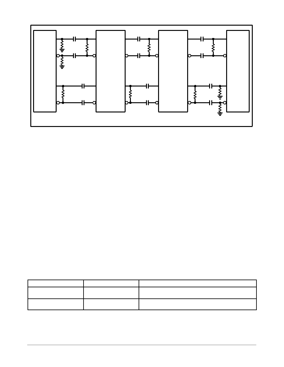
Figure 5. NB4N7132 Application Interface Example
NB4N7132
SerDes
TX+
TX
RX+
RX
O1+
O1
I1+
I1
I+
I
O+
O
O+
O
I+
I
I1+
I1
O1+
O1
RX+
RX
TX+
TX
0.01mF
R
RT
“R” is 150 W for both 100 W differential or 150 W differential traces.
“RT” matches the differential impedance of the link.
R
IN+/IN Input Functionality
The differential inputs are internally biased to
Y1.2 V. In
a typical application, the differential inputs are
capacitorcoupled and will swing symmetrically above and
below 1.2 V, preserving a 50% duty cycle to the outputs.
With this technique, the NB4N7132 will accept any
differential input allowing for LVPECL, CML, LVDS, and
HSTL input levels.
OUT+ / OUT Outputs
The OUT+ and OUT outputs of the NB4N7132 are
designed to drive differential transmission lines with
nominally 50
W or 75 W characteristic impedance. These
differential output buffers utilize positive emitter coupled
logic (PECL) architecture, but they do not require DC output
load resistors, and will operate properly with or without the
resistors.
OEx Output Enable
The NB4N7132 incorporates output enable pins, OE0 and
OE1, that work by powering down the output buffer and
associated driving circuitry. Using this approach results in
both differential outputs going HIGH, and a reduction in IDD
current of approx. 29 mA for each disabled output pair.
When OEx is LOW, outputs are disabled, OUTx+ and
OUTx are set HIGH.
Power Supply Bypass information
A clean power supply will optimize the performance of
the device. The NB4N7132 provides separate power supply
pins for the digital circuitry (VDD) and LVPECL outputs
(VDDPn). Placing a bypass capacitor of 0.01
mF to 0.1 mF
on each VDD pin will help ensure a noise free VDD power
supply. The purpose of this design technique is to try and
isolate the high switching noise of the digital outputs from
the relatively sensitive digital core logic.
Resource Reference of Application Notes
AND8002
Marking and Date Codes
AND8009
ECLinPS Plus Spice I/O Model Kit
ORDERING INFORMATION
Device
Package
Shipping
NB4N7132DTG
TSSOP28
(PbFree)
50 Units / Rail
NB4N7132DTR2G
TSSOP28
(PbFree)
2500 / Tape & Reel
For information on tape and reel specifications, including part orientation and tape sizes, please refer to our Tape and Reel Packaging
Specifications Brochure, BRD8011/D.
相关PDF资料 |
PDF描述 |
|---|---|
| NB4N1158DTR2G | IC LINK REPLICATOR SER 28-TSSOP |
| MS27472E24B4SA | CONN RCPT 56POS WALL MT W/SCKT |
| 74CBTLV3861PW,118 | IC BUS SWITCH 10BIT 24TSSOP |
| CS3102A-32-59P | CONN RCPT 42POS BOX MNT W/PINS |
| EL5001IREZ | IC CLOCK DRIVER 6-CHAN 20-HTSSOP |
相关代理商/技术参数 |
参数描述 |
|---|---|
| NB4N840M | 制造商:ONSEMI 制造商全称:ON Semiconductor 功能描述:3.3V 3.2Gb/s Dual Differential Clock/Data 2 x 2 Crosspoint Switch with CML Output and Internal Termination |
| NB4N840M_07 | 制造商:ONSEMI 制造商全称:ON Semiconductor 功能描述:3.3V 3.2Gb/s Dual Differential Clock/Data 2 x 2 Crosspoint Switch with CML Output and Internal Termination |
| NB4N840MMNEVB | 功能描述:BOARD EVAL BBG NB4N840MMN RoHS:是 类别:编程器,开发系统 >> 评估演示板和套件 系列:* 标准包装:1 系列:PCI Express® (PCIe) 主要目的:接口,收发器,PCI Express 嵌入式:- 已用 IC / 零件:DS80PCI800 主要属性:- 次要属性:- 已供物品:板 |
| NB4N840MMNG | 功能描述:模拟和数字交叉点 IC ANA 2X2 CROSSPT SWCH CML RoHS:否 制造商:Micrel 配置:2 x 2 封装 / 箱体:MLF-16 数据速率:10.7 Gbps 输入电平:CML, LVDS, LVPECL 输出电平:CML 电源电压-最大:3.6 V 电源电压-最小:2.375 V 最大工作温度:+ 85 C 最小工作温度:- 40 C 产品:Digital Crosspoint 封装:Tube |
| NB4N840MMNR4G | 功能描述:模拟和数字交叉点 IC ANA 2X2 CROSSPT SWCH CML RoHS:否 制造商:Micrel 配置:2 x 2 封装 / 箱体:MLF-16 数据速率:10.7 Gbps 输入电平:CML, LVDS, LVPECL 输出电平:CML 电源电压-最大:3.6 V 电源电压-最小:2.375 V 最大工作温度:+ 85 C 最小工作温度:- 40 C 产品:Digital Crosspoint 封装:Tube |
发布紧急采购,3分钟左右您将得到回复。