参数资料
| 型号: | NB6L11DTR2 |
| 厂商: | ON Semiconductor |
| 文件页数: | 9/13页 |
| 文件大小: | 0K |
| 描述: | IC CLK BUFFER TRANSLA 1:2 8TSSOP |
| 产品变化通告: | Product Discontinuation 20/Aug/2008 |
| 标准包装: | 2,500 |
| 类型: | 扇出缓冲器(分配),变换器 |
| 电路数: | 1 |
| 比率 - 输入:输出: | 1:2 |
| 差分 - 输入:输出: | 是/是 |
| 输入: | CML,LVCMOS,LVDS,LVNECL,LVPECL,LVTTL |
| 输出: | ECL |
| 频率 - 最大: | 6GHz |
| 电源电压: | 2.375 V ~ 3.465 V |
| 工作温度: | -40°C ~ 85°C |
| 安装类型: | 表面贴装 |
| 封装/外壳: | 8-TSSOP,8-MSOP(0.118",3.00mm 宽) |
| 供应商设备封装: | 8-TSSOP |
| 包装: | 带卷 (TR) |
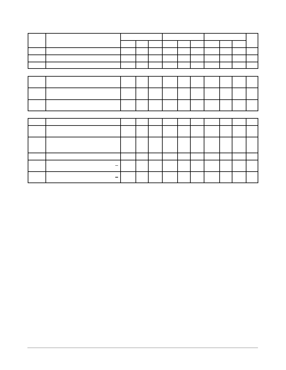
NB6L11
http://onsemi.com
5
Symbol
Characteristic
40°C
25°C
85°C
Unit
Min
Typ
Max
Min
Typ
Max
Min
Typ
Max
IEE
Negative Power Supply Current (Note 12)
5
14
20
5
14
20
5
14
20
mA
VOH
Output HIGH Voltage (Note 13)
2150
2250
2350
2200
2300
2400
2250
2350
2450
mV
VOL
Output LOW Voltage (Note 13)
1365
1525
1670
1430
1565
1720
1490
1625
1770
mV
Vth
Input Threshold Reference Voltage Range
(Note 9)
1125
VCC
75
1125
VCC
75
1125
VCC
75
mV
VIH
SingleEnded Input HIGH Voltage
Vth
+75
VCC
Vth
+75
VCC
Vth
+75
VCC
mV
VIL
SingleEnded Input LOW Voltage
VEE
Vth
75
VEE
Vth
75
VEE
Vth
75
mV
VIHD
Differential Input HIGH Voltage
1200
VCC
1200
VCC
1200
VCC
mV
VILD
Differential Input LOW Voltage
VEE
VCC
75
VEE
VCC
75
VEE
VCC
75
mV
VCMR
Input Common Mode Range
(Differential CrossPoint Voltage)
(Note 10)
950
VCC
38
950
VCC
38
950
VCC
38
mV
VID
Differential Input Voltage (VIHD VILD)
75
2500
75
2500
75
2500
mV
IIH
Input HIGH Current
D
50
10
150
50
10
150
50
10
150
mA
IIL
Input LOW Current
D
150
5
30
150
5
30
150
5
30
mA
NOTE: Device will meet the specifications after thermal equilibrium has been established when mounted in a test socket or printed circuit
board with maintained transverse airflow greater than 500 lfpm. Electrical parameters are guaranteed only over the declared
operating temperature range. Functional operation of the device exceeding these conditions is not implied. Device specification
limit values are applied individually under normal operating conditions and not valid simultaneously.
9. Vth is applied to the complementary input when operating in singleended mode.
10.VCMR minimum varies 1:1 with VEE, VCMR maximum varies 1:1 with VCC.
11. Input and output parameters vary 1:1 with VCC. VEE can vary +0.3 V to 2.2 V.
12.All input and output pins left open.
13.All loading with 50 W to VCC 2.0 V.
14.Vth, VIH, and VIL parameters must be complied with simultaneously.
15.VIHD, VILD, VID and VCMR parameters must be complied with simultaneously.
相关PDF资料 |
PDF描述 |
|---|---|
| NB6L11SMNR2G | IC CLK BUFFER TRANSLA 1:2 16-QFN |
| NB6L14MNG | IC CLOCK BUFFER 1:4 3GHZ 16-QFN |
| NB6L14MNR2G | IC CLOCK BUFFER 1:4 3GHZ 16-QFN |
| NB6L14SMNTWG | IC CLK BUFFER TRANSLA 1:4 16-QFN |
| NB6L16DTR2 | IC CLK BUFF DRIVER XLATOR 8TSSOP |
相关代理商/技术参数 |
参数描述 |
|---|---|
| NB6L11DTR2G | 功能描述:时钟缓冲器 2.5V/3.3V Multilevel 1:2 Clock / Fanout RoHS:否 制造商:Texas Instruments 输出端数量:5 最大输入频率:40 MHz 传播延迟(最大值): 电源电压-最大:3.45 V 电源电压-最小:2.375 V 最大功率耗散: 最大工作温度:+ 85 C 最小工作温度:- 40 C 封装 / 箱体:LLP-24 封装:Reel |
| NB6L11M | 制造商:ONSEMI 制造商全称:ON Semiconductor 功能描述:2.5V / 3.3V 1:2 Differential CML Fanout Buffer |
| NB6L11M_07 | 制造商:ONSEMI 制造商全称:ON Semiconductor 功能描述:2.5V / 3.3V 1:2 Differential CML Fanout Buffer Multi−Level Inputs w/ Internal Termination |
| NB6L11MMNG | 功能描述:时钟缓冲器 1:2 CML FANOUT RoHS:否 制造商:Texas Instruments 输出端数量:5 最大输入频率:40 MHz 传播延迟(最大值): 电源电压-最大:3.45 V 电源电压-最小:2.375 V 最大功率耗散: 最大工作温度:+ 85 C 最小工作温度:- 40 C 封装 / 箱体:LLP-24 封装:Reel |
| NB6L11MMNGEVB | 功能描述:电源管理IC开发工具 NB6L11MMNG EVAL BOARD RoHS:否 制造商:Maxim Integrated 产品:Evaluation Kits 类型:Battery Management 工具用于评估:MAX17710GB 输入电压: 输出电压:1.8 V |
发布紧急采购,3分钟左右您将得到回复。