参数资料
| 型号: | NB6L56MNG |
| 厂商: | ON Semiconductor |
| 文件页数: | 7/10页 |
| 文件大小: | 0K |
| 描述: | IC MUX 2.5V/3.3V DUAL DIFF 32QFN |
| 标准包装: | 74 |
| 系列: | ECLinPS MAX™ |
| 类型: | 扇出缓冲器(分配),多路复用器,数据 |
| 电路数: | 2 |
| 比率 - 输入:输出: | 2:1 |
| 差分 - 输入:输出: | 是/是 |
| 输入: | CML,LVDS,LVPECL |
| 输出: | LVPECL |
| 频率 - 最大: | 2.5GHz |
| 电源电压: | 2.375 V ~ 3.6 V |
| 工作温度: | -40°C ~ 85°C |
| 安装类型: | 表面贴装 |
| 封装/外壳: | 32-VFQFN 裸露焊盘 |
| 供应商设备封装: | 32-QFN(5x5) |
| 包装: | 管件 |
NB6L56
http://onsemi.com
6
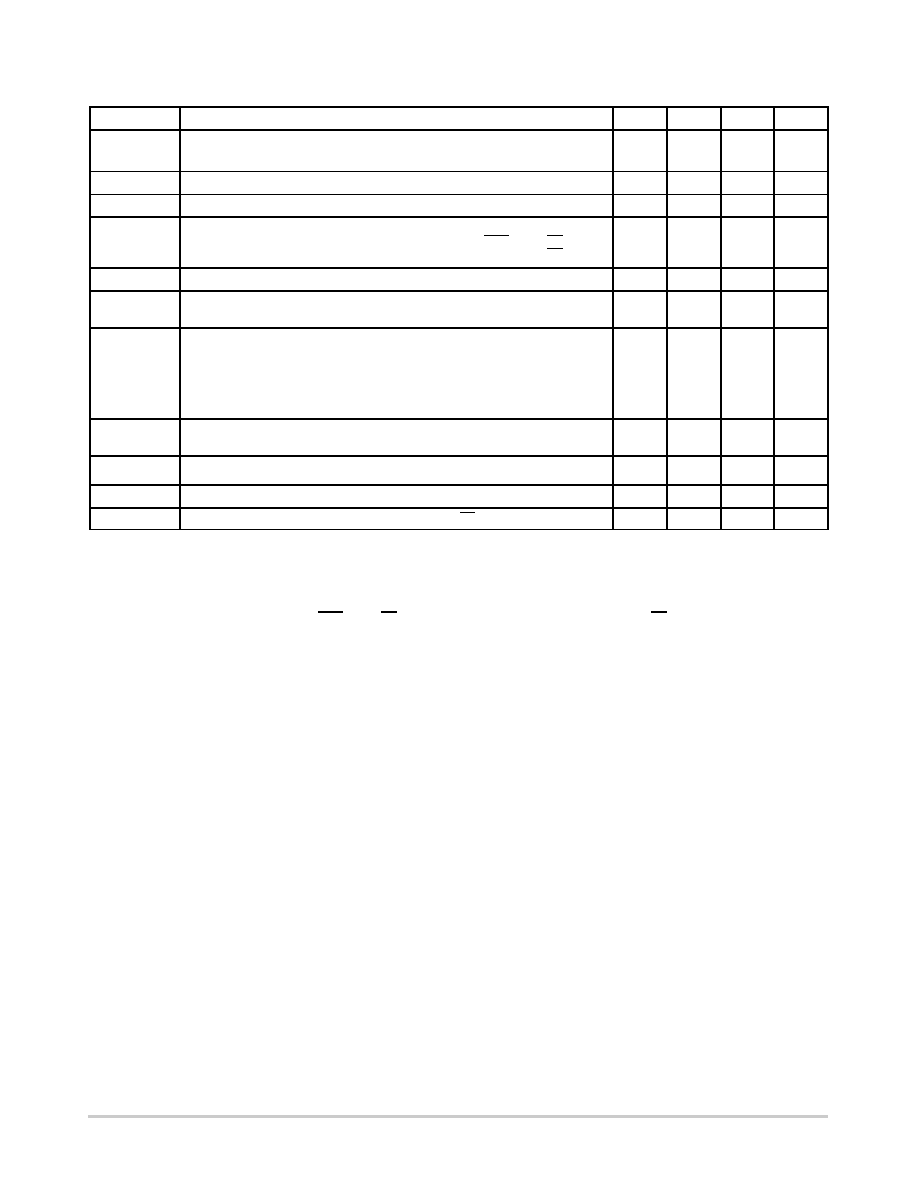
Table 6. AC CHARACTERISTICS VCC = 2.5 ± 5% (2.375 V to 2.625 V); VCC = 3.3 ± 10% (3.0 V to 3.6 V) (Note 8)
Symbol
Characteristic
Min
Typ
Max
Unit
fMAX
Maximum Input Clock Frequency
Voutpp w 400 mV
Maximum Operating Data Rate (NRZ)
Voutpp w 400 mV
2.5
Ghz
Gbps
fSEL
Maximum Toggle Frequency, SELA/SELB
25
50
MHz
VOUTPP
Output Voltage Amplitude (Differential Interconnect) fin ≤ 2.5 GHz
400
mVpp
tPLH,
tPHL
Propagation Delay to Differential Outputs, @ 1 GHz,
INxn/INxn to Qx, Qx
SELx to Qx, Qx
160
100
250
260
360
400
ps
tPLH Tempco
Differential Propagation Delay Temperature Coefficient
143
Dfs/°C
tskew
Input to Input per Bank Within Device
Output Bank to Output Bank Within Device
10
12
20
25
ps
tJITTER
DATA JITTER
RJ for K28.7 at 2.5 GHz (RMS)
DJ for NRZ PRBS23 / K28.5 at 2.5 Gbps
CLOCK JITTER
Cycle to Cycle (1K WFMS; RMS)
Total Jitter TJ (PP)
1
10
1
10
ps
tjit(f)
Integrated Phase Jitter fin = 155.52 MHz and 1GHz 12 kHz * 20 MHz Offset
(RMS)
35
fs
tJITTER
Crosstalk Induced Jitter Input to Input per Output Bank Within Device (Note 9)
0.7
psRMS
VINPP
Input Voltage Swing (Differential Configuration) (Note 10)
100
1200
mV
tr,, tf
Output Rise/Fall Times @ 1 GHz (20% 80%), Qx, Qx
50
100
180
ps
NOTE: Device will meet the specifications after thermal equilibrium has been established when mounted in a test socket or printed circuit
board with maintained transverse airflow greater than 500 lfpm. Electrical parameters are guaranteed only over the declared
operating temperature range. Functional operation of the device exceeding these conditions is not implied. Device specification limit
values are applied individually under normal operating conditions and not valid simultaneously.
8. Differential 50% duty cycle at VINPPmin clock source. Outputs evaluated with 50 W resistors to VTT = VCC 2.0 V (See Figure 16). Input
crosspoint to output crosspoint for INxn/INxn to Qx, Qx; 50% input to output crosspoint for SELx to Qx, Qx. See Figures 5, 10 and 11.
9. Crosstalk is measured at the output while applying two similar clock frequencies that are asynchronous with respect to each other at the
inputs.
10.Input voltage swing is a singleended measurement operating in differential mode.
相关PDF资料 |
PDF描述 |
|---|---|
| NB6L572MMNG | IC CLK BUFF MUX XLATOR 4:2 32QFN |
| NB6L611MNR2G | IC CLOCK BUFFER 1:2 4GHZ 16-QFN |
| NB6LQ572MMNG | IC CLK BUFFER MUX TRANSLA 32-QFN |
| NB6LQ572MNG | IC CLOCK MUX TRANSLA 4:2 32-QFN |
| NB6N11SMNR2G | IC CLK BUFFER TRANSLA 1:2 16-QFN |
相关代理商/技术参数 |
参数描述 |
|---|---|
| NB6L56MNTXG | 功能描述:时钟缓冲器 2.5V/3.3V DUAL DIFFERENTI RoHS:否 制造商:Texas Instruments 输出端数量:5 最大输入频率:40 MHz 传播延迟(最大值): 电源电压-最大:3.45 V 电源电压-最小:2.375 V 最大功率耗散: 最大工作温度:+ 85 C 最小工作温度:- 40 C 封装 / 箱体:LLP-24 封装:Reel |
| NB6L572M | 制造商:ONSEMI 制造商全称:ON Semiconductor 功能描述:2.5V / 3.3V Differential 4:1 Mux to 1:2 CML Clock/Data Fanout / Translator |
| NB6L572MMNG | 功能描述:编码器、解码器、复用器和解复用器 ANA 500MA ANY CAP LDO RoHS:否 制造商:Micrel 产品:Multiplexers 逻辑系列:CMOS 位数: 线路数量(输入/输出):2 / 12 传播延迟时间:350 ps, 400 ps 电源电压-最大:2.625 V, 3.6 V 电源电压-最小:2.375 V, 3 V 最大工作温度:+ 85 C 安装风格:SMD/SMT 封装 / 箱体:QFN-44 封装:Tray |
| NB6L572MMNR4G | 制造商:ON Semiconductor 功能描述:2.5/3.3V 4:1 DIFF MUX - Tape and Reel |
| NB6L611 | 制造商:ONSEMI 制造商全称:ON Semiconductor 功能描述:2.5V / 3.3V 1:2 Differential LVPECL Clock / Data Fanout Buffer |
发布紧急采购,3分钟左右您将得到回复。