参数资料
| 型号: | NB6L611MNG |
| 厂商: | ON Semiconductor |
| 文件页数: | 3/10页 |
| 文件大小: | 0K |
| 描述: | IC CLOCK BUFFER 1:2 4GHZ 16-QFN |
| 标准包装: | 123 |
| 系列: | ECLinPS MAX™ |
| 类型: | 扇出缓冲器(分配) |
| 电路数: | 1 |
| 比率 - 输入:输出: | 1:2 |
| 差分 - 输入:输出: | 是/是 |
| 输入: | CML,LVCMOS,LVDS,LVPECL,LVTTL |
| 输出: | LVPECL |
| 频率 - 最大: | 4GHz |
| 电源电压: | 2.375 V ~ 3.63 V |
| 工作温度: | -40°C ~ 85°C |
| 安装类型: | 表面贴装 |
| 封装/外壳: | 16-VFQFN 裸露焊盘 |
| 供应商设备封装: | 16-QFN(3x3) |
| 包装: | 管件 |
| 其它名称: | NB6L611MNG-ND NB6L611MNGOS |
NB6L611
http://onsemi.com
2
VCC VREFAC VEE VCC
VCC VEE VEE VCC
Q0
Q1
VTD
D
VTD
56
7
8
16
15
14
13
12
11
10
9
1
2
3
4
NB6L611
Exposed Pad (EP)
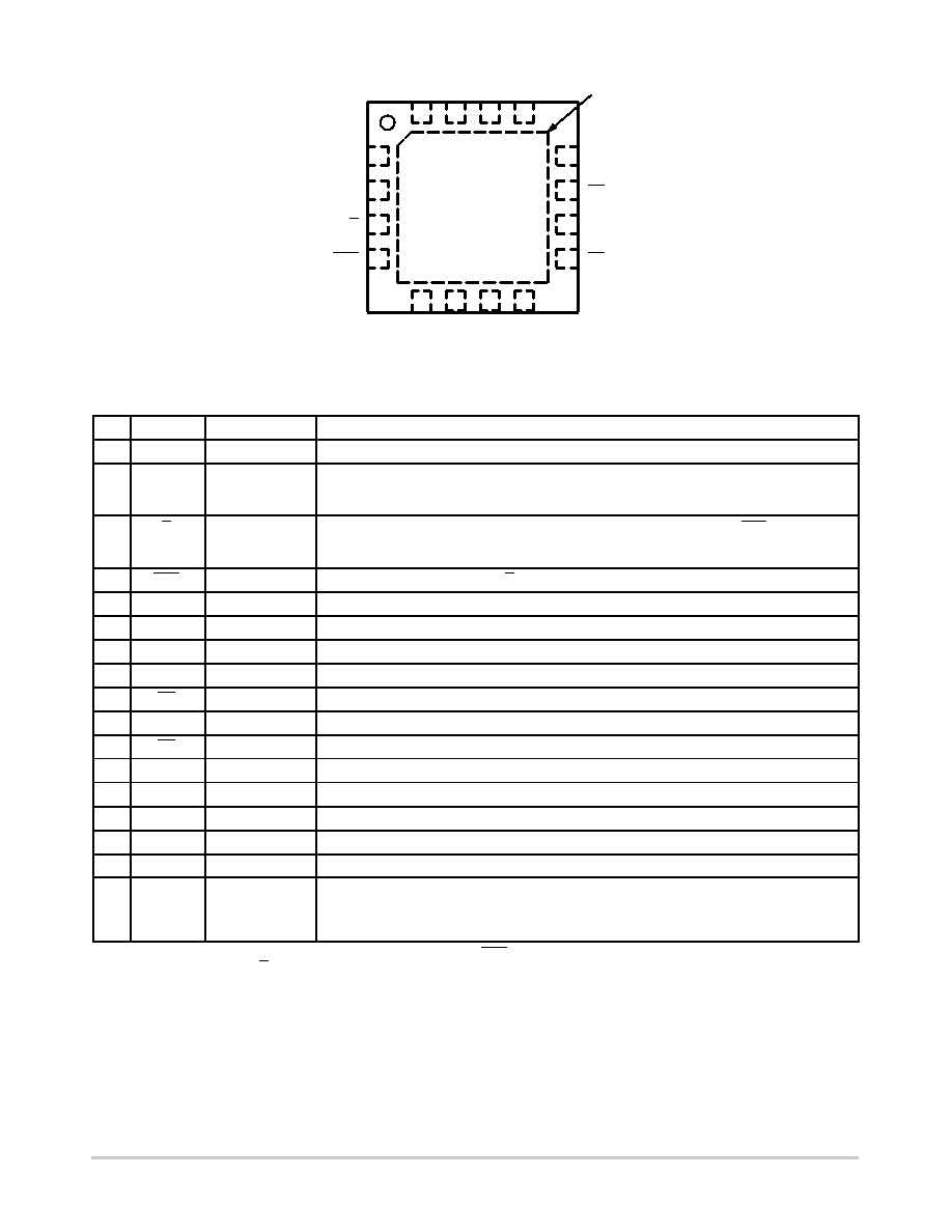
Figure 2. Pin Configuration (Top View)
Table 1. PIN DESCRIPTION
Pin
Name
I/O
Description
1
VTD
Internal 50 W Termination Pin for D input.
2
D
ECL, CML,
LVCMOS, LVDS,
LVTTL Input
Noninverted Differential Input. Note1. Internal 50 W Resistor to Termination Pin, VTD.
3
D
ECL, CML,
LVCMOS, LVDS,
LVTTL Input
Inverted Differential Input. Note 1. Internal 50 W Resistor to Termination Pin, VTD.
4
VTD
Internal 50 W Termination Pin for D input.
5
VCC
Positive Supply Voltage
6
VREFAC
Output Reference Voltage for direct or capacitor coupled inputs
7
VEE
Negative Supply Voltage
8
VCC
Positive Supply Voltage
9
Q1
LVPECL Output
Inverted Differential Output. Typically Terminated with 50 W Resistor to VCC 2.0 V.
10
Q1
LVPECL Output
Noninverted Differential Output. Typically Terminated with 50 W Resistor to VCC 2.0 V.
11
Q0
LVPECL Output
Inverted Differential Output. Typically Terminated with 50 W Resistor to VCC 2.0 V.
12
Q0
LVPECL Output
Noninverted Differential Output. Typically Terminated with 50 W Resistor to VCC 2.0 V.
13
VCC
Positive Supply Voltage
14
VEE
Negative Supply Voltage
15
VEE
Negative Supply Voltage
16
VCC
Positive Supply Voltage
EP
The Exposed Pad (EP) on the QFN16 package bottom is thermally connected to the die for
improved heat transfer out of package. The exposed pad must be attached to a heatsinking
conduit. The pad is not electrically connected to the die, but is recommended to be electrically
and thermally connected to VEE on the PC board.
1. In the differential configuration when the input termination pins (VTD, VTD) are connected to a common termination voltage or left open, and
if no signal is applied on D/D input, then, the device will be susceptible to selfoscillation.
2. All VCC and VEE pins must be externally connected to a power supply for proper operation.
相关PDF资料 |
PDF描述 |
|---|---|
| LTC2621CDD#TRPBF | IC DAC 12BIT SGL R-R VOUT 10DFN |
| VI-21V-MW-F4 | CONVERTER MOD DC/DC 5.8V 100W |
| NB6N14SMNG | IC CLK BUFFER TRANSLA 1:4 16-QFN |
| LTC2621CDD#TR | IC DAC 12BIT SGL R-R VOUT 10DFN |
| MC100EP11DG | IC CLOCK BUFFER 1:2 3GHZ 8-SOIC |
相关代理商/技术参数 |
参数描述 |
|---|---|
| NB6L611MNGEVB | 功能描述:BOARD EVAL NB6L611MNG RoHS:是 类别:编程器,开发系统 >> 评估演示板和套件 系列:* 产品培训模块:Obsolescence Mitigation Program 标准包装:1 系列:- 主要目的:电源管理,电池充电器 嵌入式:否 已用 IC / 零件:MAX8903A 主要属性:1 芯锂离子电池 次要属性:状态 LED 已供物品:板 |
| NB6L611MNR2G | 功能描述:时钟缓冲器 1:2 PECL FANOUT RoHS:否 制造商:Texas Instruments 输出端数量:5 最大输入频率:40 MHz 传播延迟(最大值): 电源电压-最大:3.45 V 电源电压-最小:2.375 V 最大功率耗散: 最大工作温度:+ 85 C 最小工作温度:- 40 C 封装 / 箱体:LLP-24 封装:Reel |
| NB6L72 | 制造商:ONSEMI 制造商全称:ON Semiconductor 功能描述:2.5V / 3.3V Differential 2 X 2 Crosspoint Switch with LVPECL Outputs |
| NB6L72M | 制造商:ONSEMI 制造商全称:ON Semiconductor 功能描述:2.5V / 3.3V Differential 2 X 2 Crosspoint Switch with CML Outputs |
| NB6L72M_07 | 制造商:ONSEMI 制造商全称:ON Semiconductor 功能描述:2.5V / 3.3V Differential 2 X 2 Crosspoint Switch with CML Outputs |
发布紧急采购,3分钟左右您将得到回复。