参数资料
| 型号: | NB6L611MNG |
| 厂商: | ON Semiconductor |
| 文件页数: | 6/10页 |
| 文件大小: | 0K |
| 描述: | IC CLOCK BUFFER 1:2 4GHZ 16-QFN |
| 标准包装: | 123 |
| 系列: | ECLinPS MAX™ |
| 类型: | 扇出缓冲器(分配) |
| 电路数: | 1 |
| 比率 - 输入:输出: | 1:2 |
| 差分 - 输入:输出: | 是/是 |
| 输入: | CML,LVCMOS,LVDS,LVPECL,LVTTL |
| 输出: | LVPECL |
| 频率 - 最大: | 4GHz |
| 电源电压: | 2.375 V ~ 3.63 V |
| 工作温度: | -40°C ~ 85°C |
| 安装类型: | 表面贴装 |
| 封装/外壳: | 16-VFQFN 裸露焊盘 |
| 供应商设备封装: | 16-QFN(3x3) |
| 包装: | 管件 |
| 其它名称: | NB6L611MNG-ND NB6L611MNGOS |
NB6L611
http://onsemi.com
5
Table 5. AC CHARACTERISTICS VCC = 2.375 V to 3.63 V, VEE = 0 V, or VCC = 0 V, VEE = 2.375 V to 3.63 V,
Symbol
Characteristic
Min
Typ
Max
Unit
VOUTPP Output Voltage Amplitude (@ VINPP)fin ≤ 1.5 GHz
fin = 2.0 GHz
fin = 3.0 GHz
fin = 4.0 GHz
725
520
320
170
780
680
500
400
mV
tPD
Propagation Delay
D to Q
225
280
375
ps
tSKEW
Duty Cycle Skew (Note 11)
Within Device Skew
Device to Device Skew (Note 12)
3
15
80
ps
tDC
Output Clock Duty Cycle
fin ≤ 4.0 GHz
(Reference Duty Cycle = 50%)
40
50
60
ps
tJITTER
RMS Random Clock Jitter (Note 13)
fin ≤ 4.0 GHz
0.2
0.5
ps
VINPP
Input Voltage Swing/Sensitivity
(Differential Configuration) (Note 14)
150
VCC VEE
mV
tr,tf
Output Rise/Fall Times @ 0.5 GHz (20% 80%)
Q, Q
100
170
ps
NOTE: Device will meet the specifications after thermal equilibrium has been established when mounted in a test socket or printed circuit
board with maintained transverse airflow greater than 500 lfpm. Electrical parameters are guaranteed only over the declared
operating temperature range. Functional operation of the device exceeding these conditions is not implied. Device specification limit
values are applied individually under normal operating conditions and not valid simultaneously.
10.Measured by forcing VINPP (MIN) from a 50% duty cycle clock source. All loading with an external RL = 50 W to VCC 2.0 V. Input edge rates
40 ps (20% 80%).
11. Duty cycle skew is measured between differential outputs using the deviations of the sum of Tpw and Tpw+ @ 0.5GHz.
12.Device to device skew is measured between outputs under identical transition @ 0.5 GHz.
13.Additive RMS jitter with 50% duty cycle clock signal.
14.Input and output voltage swing is a singleended measurement operating in differential mode.
800
700
600
500
400
300
200
100
0
01
23
fout, CLOCK OUTPUT FREQUENCY (GHz)
V
OUTP
P
OUTPUT
VOL
TAGE
AMPLITUDE
(mV)
(TYPICAL)
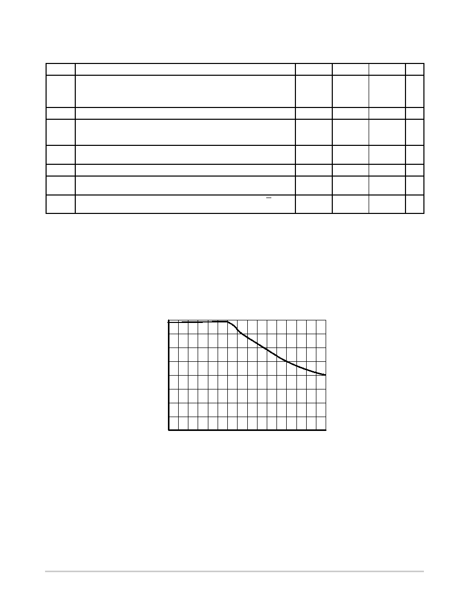
Figure 3. Output Voltage Amplitude (VOUTPP) versus Output
Frequency at Ambient Temperature (Typical)
4
相关PDF资料 |
PDF描述 |
|---|---|
| LTC2621CDD#TRPBF | IC DAC 12BIT SGL R-R VOUT 10DFN |
| VI-21V-MW-F4 | CONVERTER MOD DC/DC 5.8V 100W |
| NB6N14SMNG | IC CLK BUFFER TRANSLA 1:4 16-QFN |
| LTC2621CDD#TR | IC DAC 12BIT SGL R-R VOUT 10DFN |
| MC100EP11DG | IC CLOCK BUFFER 1:2 3GHZ 8-SOIC |
相关代理商/技术参数 |
参数描述 |
|---|---|
| NB6L611MNGEVB | 功能描述:BOARD EVAL NB6L611MNG RoHS:是 类别:编程器,开发系统 >> 评估演示板和套件 系列:* 产品培训模块:Obsolescence Mitigation Program 标准包装:1 系列:- 主要目的:电源管理,电池充电器 嵌入式:否 已用 IC / 零件:MAX8903A 主要属性:1 芯锂离子电池 次要属性:状态 LED 已供物品:板 |
| NB6L611MNR2G | 功能描述:时钟缓冲器 1:2 PECL FANOUT RoHS:否 制造商:Texas Instruments 输出端数量:5 最大输入频率:40 MHz 传播延迟(最大值): 电源电压-最大:3.45 V 电源电压-最小:2.375 V 最大功率耗散: 最大工作温度:+ 85 C 最小工作温度:- 40 C 封装 / 箱体:LLP-24 封装:Reel |
| NB6L72 | 制造商:ONSEMI 制造商全称:ON Semiconductor 功能描述:2.5V / 3.3V Differential 2 X 2 Crosspoint Switch with LVPECL Outputs |
| NB6L72M | 制造商:ONSEMI 制造商全称:ON Semiconductor 功能描述:2.5V / 3.3V Differential 2 X 2 Crosspoint Switch with CML Outputs |
| NB6L72M_07 | 制造商:ONSEMI 制造商全称:ON Semiconductor 功能描述:2.5V / 3.3V Differential 2 X 2 Crosspoint Switch with CML Outputs |
发布紧急采购,3分钟左右您将得到回复。