参数资料
| 型号: | NB7L216MNR2 |
| 厂商: | ON Semiconductor |
| 文件页数: | 1/11页 |
| 文件大小: | 0K |
| 描述: | IC RECEIVER/DRIVER DIFF 16-QFN |
| 标准包装: | 3,000 |
| 逻辑类型: | 差分接收器/驱动器 |
| 电源电压: | 2.375 V ~ 3.465 V |
| 工作温度: | -40°C ~ 85°C |
| 安装类型: | 表面贴装 |
| 封装/外壳: | 16-VFQFN 裸露焊盘 |
| 供应商设备封装: | 16-QFN(3x3) |
| 包装: | 带卷 (TR) |
Semiconductor Components Industries, LLC, 2009
August, 2009 Rev. 5
1
Publication Order Number:
NB7L216/D
NB7L216
2.5V/3.3V, 12Gb/s Multi
Level Clock/Data Input to
RSECL, High Gain
Receiver/Buffer/Translator
with Internal Termination
Description
The NB7L216 is a differential receiver/driver with high gain output
targeted for high frequency applications. The device is functionally
equivalent to the NBSG16 but with much higher gain output. This
highly versatile device provides 35 dB of gain up to 7 GHz.
Inputs incorporate internal 50
W termination resistors and accept
Negative ECL (NECL), Positive ECL (PECL), LVTTL, LVCMOS,
CML, or LVDS. Outputs are Reduced Swing ECL (RSECL), 400 mV.
The VBB pin is an internally generated voltage supply available to
this device only. VBB is used as a reference voltage for singleended
NECL or PECL inputs. For all singleended input conditions, the
unused complementary differential input should be connected to VBB
as a switching reference voltage. VBB may also rebias AC coupled
inputs. When used, decouple VBB via a 0.01 mF capacitor and limit
current sourcing or sinking to 0.5 mA. When not used, VBB output
should be left open.
Application notes, models and support documentation are available
at www.onsemi.com.
Features
High Gain of 35 dB from DC to 7 GHz Typical
High IIP3: 0 dBm Typical
20 mV Minimum Input Voltage Swing
Maximum Input Clock Frequency up to 8.5 GHz
Maximum Input Data Rate up to 12 Gb/s Typical
<0.5 ps of RMS Clock Jitter
<9 ps of Data Dependent Jitter
120 ps Typical Propagation Delay
30 ps Typical Rise and Fall Times
RSPECL Output with Operating Range: VCC = 2.375 V to 3.465 V
with VEE = 0 V
RSNECL Output with RSNECL or NECL Inputs with Operating
Range: VCC = 0 V with VEE = 2.375 V to 3.465 V
RSECL Output Level (400 mV PeaktoPeak Output),
50 W Internal Input Termination Resistors (TemperatureCoefficient
of < 6.38 m
W/°C)
VBB – ECL Reference Voltage Output
PbFree Packages are Available
50 W
VTD
D
VTD
Q
QFN16
MN SUFFIX
CASE 485G
MARKING DIAGRAM*
*For additional marking information, refer to
Application Note AND8002/D.
A
= Assembly Location
L
= Wafer Lot
Y
= Year
W
= Work Week
G
= PbFree Package
See detailed ordering and shipping information in the package
dimensions section on page 10 of this data sheet.
ORDERING INFORMATION
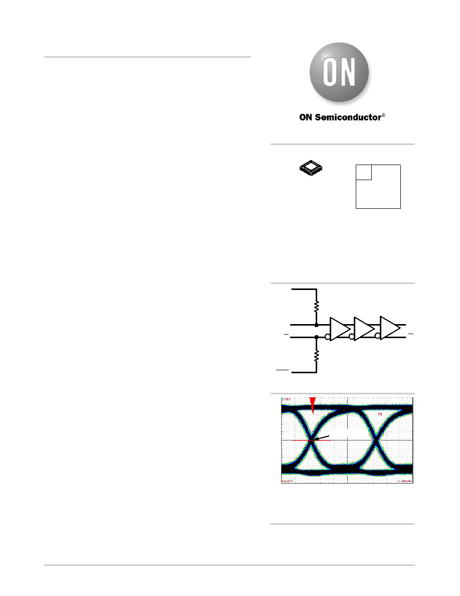
Figure 1. Functional Block Diagram
TIME (17 ps/div)
Figure 2. Typical Output Waveform at
12 Gb/s with PRBS 2231 (VINPP = 400 mV,
Input Signal DDJ = 12 ps)
VOL
TAGE
(60
mV/div)
http://onsemi.com
Device DDJ = 3 ps
(Note: Microdot may be in either location)
1
16
NB7L
216
ALYWG
G
1
相关PDF资料 |
PDF描述 |
|---|---|
| NB7L32MMNG | IC CLOCK DIVIDER 1:2 16-QFN |
| NB7L572MNR4G | IC CLK MUX XLATOR 4:2 8GHZ 32QFN |
| NB7L585MNG | IC CLK/DATA BUFFER MUX 1:6 32QFN |
| NB7L585RMNG | IC CLK/DATA BUFFER MUX 1:6 32QFN |
| NB7L86MMNR2 | IC GATE MULTI FUNCT DIFF 16-QFN |
相关代理商/技术参数 |
参数描述 |
|---|---|
| NB7L216MNR2G | 功能描述:转换 - 电压电平 2.5V/3.3V Diff RCVR w/High Gain RoHS:否 制造商:Micrel 类型:CML/LVDS/LVPECL to LVCMOS/LVTTL 传播延迟时间:1.9 ns 电源电流:14 mA 电源电压-最大:3.6 V 电源电压-最小:3 V 最大工作温度:+ 85 C 安装风格:SMD/SMT 封装 / 箱体:MLF-8 |
| NB7L32M | 制造商:ONSEMI 制造商全称:ON Semiconductor 功能描述:2.5V/3.3V, 14GHz ±2 Clock Divider w/CML Output and Internal Termination |
| NB7L32MMNEVB | 功能描述:BOARD EVAL FOR NB7L32MM RoHS:是 类别:编程器,开发系统 >> 评估演示板和套件 系列:* 标准包装:1 系列:PCI Express® (PCIe) 主要目的:接口,收发器,PCI Express 嵌入式:- 已用 IC / 零件:DS80PCI800 主要属性:- 次要属性:- 已供物品:板 |
| NB7L32MMNG | 功能描述:时钟驱动器及分配 DIV BY 2 W/CML OUT RoHS:否 制造商:Micrel 乘法/除法因子:1:4 输出类型:Differential 最大输出频率:4.2 GHz 电源电压-最大: 电源电压-最小:5 V 最大工作温度:+ 85 C 封装 / 箱体:SOIC-8 封装:Reel |
| NB7L32MMNR2G | 功能描述:时钟驱动器及分配 DIV BY 2 W/CML OUT RoHS:否 制造商:Micrel 乘法/除法因子:1:4 输出类型:Differential 最大输出频率:4.2 GHz 电源电压-最大: 电源电压-最小:5 V 最大工作温度:+ 85 C 封装 / 箱体:SOIC-8 封装:Reel |
发布紧急采购,3分钟左右您将得到回复。