参数资料
| 型号: | NB7L572MNG |
| 厂商: | ON Semiconductor |
| 文件页数: | 8/11页 |
| 文件大小: | 0K |
| 描述: | IC CLK MUX XLATOR 4:2 8GHZ 32QFN |
| 标准包装: | 74 |
| 系列: | GigaComm™ |
| 类型: | 多路复用器,变换器 |
| 电路数: | 1 |
| 比率 - 输入:输出: | 4:2 |
| 差分 - 输入:输出: | 是/是 |
| 输入: | CML,LVDS,LVPECL |
| 输出: | LVPECL |
| 频率 - 最大: | 8GHz |
| 电源电压: | 2.375 V ~ 3.6 V |
| 工作温度: | -40°C ~ 85°C |
| 安装类型: | 表面贴装 |
| 封装/外壳: | 32-VFQFN 裸露焊盘 |
| 供应商设备封装: | 32-QFN(5x5) |
| 包装: | 管件 |
| 其它名称: | NB7L572MNG-ND NB7L572MNGOS |
NB7L572
http://onsemi.com
6
Symbol
Characteristic
Min
Typ
Max
Unit
fMAX
Maximum Input Clock Frequency VOUT w 400 mV
7
8
GHz
fDATAMAX
Maximum Operating Data Rate NRZ, (PRBS23)
10
11
Gbps
VOUTPP
fin ≤ 5 GHz
(Note 12)
fin ≤ 7 GHz
550
400
750
500
mV
tPLH,
tPHL
Propagation Delay to Differential Outputs
Measured at Differential CrossPoint
@ 1 GHz INx/INx to Qx/Qx (Figure 9)
@ 50 MHz SELx to Qx (Figure 10)
125
300
150
175
1000
ps
tPD Tempco Differential Propagation Delay Temperature Coefficient
115
fs/°C
tskew
Output – Output skew (within device) (Note 13)
Device – Device skew (tpd max – tpd min)
0
10
50
ps
tDC
Output Clock Duty Cycle (Reference Duty Cycle = 50%)
45
50
55
%
tJITTER
Additive Random Clock Jitter, RJ(RMS) (Note 14)
fin v 7.0 GHz
Data Dependent Jitter, DDJ (Note 15)
fin v 10 Gbps
0.5
6
0.8
15
ps rms
ps pkpk
VINPP
Input Voltage Swing (Differential Configuration) (Note 16)
100
1200
mV
tr,, tf
Output Rise/Fall Times @ 1 GHz; (20% 80%), VIN = 800 mV Q, Q
25
45
65
ps
NOTE: Device will meet the specifications after thermal equilibrium has been established when mounted in a test socket or printed circuit
board with maintained transverse airflow greater than 500 lfpm. Electrical parameters are guaranteed only over the declared
operating temperature range. Functional operation of the device exceeding these conditions is not implied. Device specification limit
values are applied individually under normal operating conditions and not valid simultaneously.
11. Measured using a 100 mVpkpk source, 50% duty cycle clock source. All output loading with external 50 W to VCC 2 V. Input edge
rates 40 ps (20% 80%).
12.Output voltage swing is a singleended measurement operating in differential mode.
13.Skew is measured between outputs under identical transitions and conditions. Duty cycle skew is defined only for differential operation when
the delays are measured from crosspoint of the inputs to the crosspoint of the outputs.
14.Additive RMS jitter with 50% duty cycle clock signal.
15.Additive PeaktoPeak data dependent jitter with input NRZ data at K28.5.
16.Input voltage swing is a singleended measurement operating in differential mode.
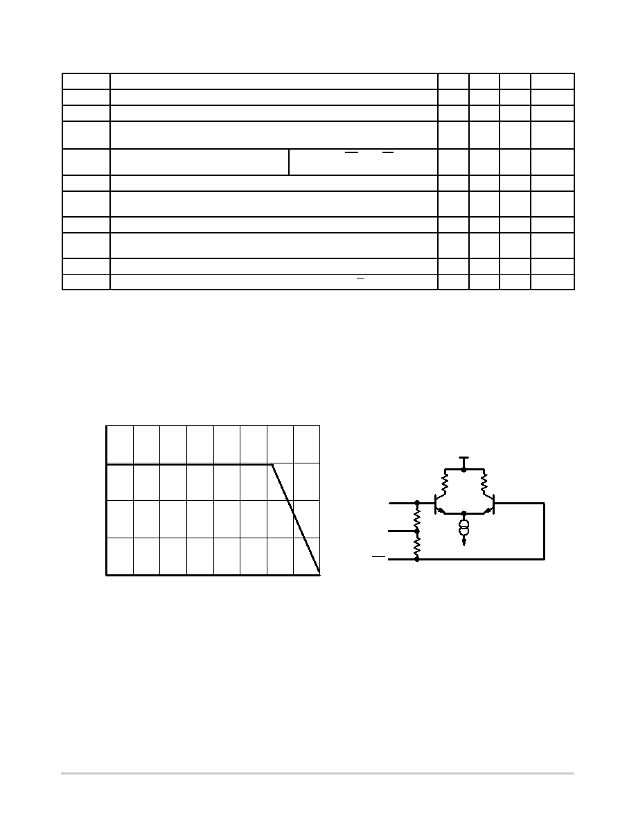
Figure 2. CLOCK Output Voltage Amplitude
(VOUTPP) / RMS Jitter vs. Input Frequency (fin) at
Ambient Temperature (typical)
fin, CLOCK INPUT FREQUENCY (GHz)
800
750
700
OUTPUT
VOL
TAGE
AMPLITUDE
(mV)
Figure 3. Input Structure
50 W
VTx
VCC
INx
01
2
8
7
6
345
650
600
相关PDF资料 |
PDF描述 |
|---|---|
| NB6L11DG | IC CLK BUFFER TRANSLA 1:2 8-SOIC |
| NB6L11DTG | IC CLK BUFFER TRANSLA 1:2 8TSSOP |
| NB6L14MMNG | IC CLOCK BUFFER 1:4 3GHZ 16-QFN |
| MC100LVEP14DTG | IC CLOCK BUFFER MUX 2:5 20-TSSOP |
| XRD54L10AIDTR-F | IC DAC 10BIT SRL LP 8SOIC |
相关代理商/技术参数 |
参数描述 |
|---|---|
| NB7L572MNR4G | 功能描述:时钟驱动器及分配 TSMC 4-1-2 MLL-PECL RoHS:否 制造商:Micrel 乘法/除法因子:1:4 输出类型:Differential 最大输出频率:4.2 GHz 电源电压-最大: 电源电压-最小:5 V 最大工作温度:+ 85 C 封装 / 箱体:SOIC-8 封装:Reel |
| NB7L585 | 制造商:ONSEMI 制造商全称:ON Semiconductor 功能描述:2.5V / 3.3V Differential 2:1 Mux Input to 1:6 LVPECL Clock/Data Fanout Buffer / Translator |
| NB7L585MNG | 功能描述:时钟驱动器及分配 2.5/3.3V DIFF MUX RoHS:否 制造商:Micrel 乘法/除法因子:1:4 输出类型:Differential 最大输出频率:4.2 GHz 电源电压-最大: 电源电压-最小:5 V 最大工作温度:+ 85 C 封装 / 箱体:SOIC-8 封装:Reel |
| NB7L585MNR4G | 功能描述:时钟驱动器及分配 2.5/3.3V DIFF MUX RoHS:否 制造商:Micrel 乘法/除法因子:1:4 输出类型:Differential 最大输出频率:4.2 GHz 电源电压-最大: 电源电压-最小:5 V 最大工作温度:+ 85 C 封装 / 箱体:SOIC-8 封装:Reel |
| NB7L585R | 制造商:ONSEMI 制造商全称:ON Semiconductor 功能描述:2.5V/3.3V, 7GHz/10Gbps Differential 2:1 Mux Input to 1:6 RSECL Clock/Data Fanout Buffer / Translator |
发布紧急采购,3分钟左右您将得到回复。