参数资料
| 型号: | NB7L86MMN |
| 厂商: | ON Semiconductor |
| 文件页数: | 5/12页 |
| 文件大小: | 0K |
| 描述: | IC GATE MULTI FUNCT DIFF 16-QFN |
| 产品变化通告: | LTB Notification 06/Feb/2008 |
| 标准包装: | 123 |
| 逻辑类型: | 可配置多功能 |
| 电路数: | 2 |
| 输入数: | 2 |
| 施密特触发器输入: | 无 |
| 输出类型: | 差分 |
| 电源电压: | 2.4 V ~ 3.5 V |
| 工作温度: | -40°C ~ 85°C |
| 安装类型: | 表面贴装 |
| 封装/外壳: | 16-VFQFN 裸露焊盘 |
| 供应商设备封装: | 16-QFN(3x3) |
| 包装: | 管件 |
NB7L86M
http://onsemi.com
2
VTD1 D1
D1 VTD1
VTD0 D0
D0 VTD0
VEE
Q
VCC
SEL
VTSEL
56
7
8
16
15
14
13
12
11
10
9
1
2
3
4
NB7L86M
Exposed Pad (EP)
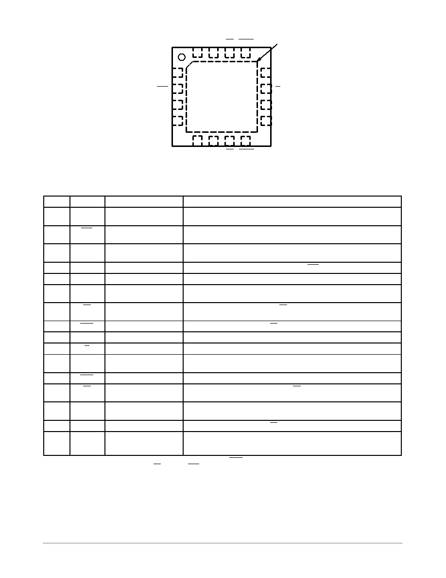
Figure 2. Pin Configuration (Top View)
Table 1. PIN DESCRIPTION
Pin
Name
I/O
Description
1, 9
VCC
Power Supply
Positive supply voltage. All VCC pins must be externally connected to power
supply to guarantee proper operation.
2
SEL
LVPECL, CML, LVCMOS,
LVTTL, LVDS Input
Inverted differential select logic input.
3
SEL
LVPECL, CML, LVCMOS,
LVTTL, LVDS Input
Noninverted differential select logic Input.
4
VTSEL
5
VTD1
6
D1
LVPECL, CML, LVCMOS,
LVTTL, LVDS Input
Noninverted differential clock/data input D1. (Note 1)
7
D1
LVPECL, CML, LVCMOS,
LVTTL, LVDS Input
Inverted differential clock/data input D1. (Note 1)
8
VTD1
10
Q
CML Output
Noninverted output with internal 50 W source termination resistor. (Note 2)
11
Q
CML Output
Inverted output with internal 50 W source termination resistor. (Note 2)
12
VEE
Power Supply
Negative supply voltage. All VEE pins must be externally connected to power
supply to guarantee proper operation.
13
VTD0
Internal 50 W termination pin for D0. (Note 1)
14
D0
LVPECL, CML, LVCMOS,
LVTTL, LVDS Input
Noninverted differential clock/data input D0. (Note 1)
15
D0
LVPECL, CML, LVCMOS,
LVTTL, LVDS Input
Noninverted differential clock/data input D0. (Note 1)
16
VTD0
Internal 50 W termination pin for D0. (Note 1)
EP
Exposed Pad. Thermal pad on the package bottom must be attached to a
heatsinking conduit to improve heat transfer. It is recommended to connect the EP
to the lower potential (VEE).
1. In the differential configuration when the input termination pins (VTDx, VTDx, VTSEL) are connected to a common termination voltage or left
open, and if no signal is applied on Dx, Dx, SEL and SEL then the device will be susceptible to selfoscillation.
2. CML output require 50 W receiver termination resistor to VCC for proper operation.
相关PDF资料 |
PDF描述 |
|---|---|
| TXR40AB45-2012AI | ADPTR TINEL LOCK ANG SHELL 21, G |
| MC14572UBD | IC GATE HEX NAND/NOR/INV 16-SOIC |
| TXR54AB90-2012BI | ADPTR TINEL LOCK ANG SHELL 20,37 |
| TXR40AB90-2014BI | ADPTR TINEL LOCK ANG SHELL 21, G |
| TXR41AB90-2014BI | ADPTR TINEL LOCK ANG SHELL 20,21 |
相关代理商/技术参数 |
参数描述 |
|---|---|
| NB7L86MMNEVB | 功能描述:BOARD EVAL BBG NB7L86MMN RoHS:是 类别:编程器,开发系统 >> 评估演示板和套件 系列:* 标准包装:1 系列:PCI Express® (PCIe) 主要目的:接口,收发器,PCI Express 嵌入式:- 已用 IC / 零件:DS80PCI800 主要属性:- 次要属性:- 已供物品:板 |
| NB7L86MMNG | 功能描述:逻辑门 2.5V/3.3V Diff Clock Data Smart Gate RoHS:否 制造商:Texas Instruments 产品:OR 逻辑系列:LVC 栅极数量:2 线路数量(输入/输出):2 / 1 高电平输出电流:- 16 mA 低电平输出电流:16 mA 传播延迟时间:3.8 ns 电源电压-最大:5.5 V 电源电压-最小:1.65 V 最大工作温度:+ 125 C 安装风格:SMD/SMT 封装 / 箱体:DCU-8 封装:Reel |
| NB7L86MMNR2 | 功能描述:逻辑门 2.5V/3.3V Diff Clock RoHS:否 制造商:Texas Instruments 产品:OR 逻辑系列:LVC 栅极数量:2 线路数量(输入/输出):2 / 1 高电平输出电流:- 16 mA 低电平输出电流:16 mA 传播延迟时间:3.8 ns 电源电压-最大:5.5 V 电源电压-最小:1.65 V 最大工作温度:+ 125 C 安装风格:SMD/SMT 封装 / 箱体:DCU-8 封装:Reel |
| NB7L86MMNR2G | 功能描述:逻辑门 2.5V/3.3V Diff Clock Data Smart Gate RoHS:否 制造商:Texas Instruments 产品:OR 逻辑系列:LVC 栅极数量:2 线路数量(输入/输出):2 / 1 高电平输出电流:- 16 mA 低电平输出电流:16 mA 传播延迟时间:3.8 ns 电源电压-最大:5.5 V 电源电压-最小:1.65 V 最大工作温度:+ 125 C 安装风格:SMD/SMT 封装 / 箱体:DCU-8 封装:Reel |
| NB7LQ572 | 制造商:ONSEMI 制造商全称:ON Semiconductor 功能描述:2.5V / 3.3V Differential 4:1 Mux w/Input Equalizer to 1:2 LVPECL Clock/Data Fanout / Translator |
发布紧急采购,3分钟左右您将得到回复。