参数资料
| 型号: | NB7L86MMN |
| 厂商: | ON Semiconductor |
| 文件页数: | 9/12页 |
| 文件大小: | 0K |
| 描述: | IC GATE MULTI FUNCT DIFF 16-QFN |
| 产品变化通告: | LTB Notification 06/Feb/2008 |
| 标准包装: | 123 |
| 逻辑类型: | 可配置多功能 |
| 电路数: | 2 |
| 输入数: | 2 |
| 施密特触发器输入: | 无 |
| 输出类型: | 差分 |
| 电源电压: | 2.4 V ~ 3.5 V |
| 工作温度: | -40°C ~ 85°C |
| 安装类型: | 表面贴装 |
| 封装/外壳: | 16-VFQFN 裸露焊盘 |
| 供应商设备封装: | 16-QFN(3x3) |
| 包装: | 管件 |
NB7L86M
http://onsemi.com
6
Symbol
Characteristic
40_C
25_C
85_C
Unit
Min
Typ
Max
Min
Typ
Max
Min
Typ
Max
VOUTPP Output Voltage Amplitude (@VINPPmin)fin ≤ 4 GHz
(See Figure 7)
fin ≤ 8 GHz
240
125
350
230
240
125
350
230
240
125
350
230
mV
fdata
Maximum Operating Data Rate
10.7
12
10.7
12
10.7
12
Gb/s
tPLH,
tPHL
Propagation Delay to
Dx/Dx to Q/Q
Output Differential @ 1 GHz
SEL/SEL to Q/Q
(See Figure 7)
70
110
90
135
120
180
70
110
90
135
120
180
70
110
90
135
120
180
ps
tSKEW
Duty Cycle Skew (Note 14)
DevicetoDevice Skew (Note 15)
2.0
5.0
10
20
2.0
5.0
10
20
2.0
5.0
10
20
ps
tS
SetUp Time (Dx to SEL)
100
ps
tH
HoldUp Time (Dx to SEL)
15
ps
tJITTER
RMS Random Clock Jitter (Note 16)
fin = 4 GHz
fin =8 GHz
Peak/Peak Data Dependent Jitter
fdata = 5 Gb/s
(Note 17)
fdata =10 Gb/s
0.2
2.0
4.0
0.5
8.0
10
0.2
2.0
4.0
0.5
8.0
10
0.2
2.0
4.0
0.5
8.0
10
ps
VINPP
Input Voltage Swing/Sensitivity
(Differential Configuration) (Note 18)
75
400
2500
75
400
2500
75
400
2500
mV
tr
tf
Output Rise/Fall Times @ 1 GHz
Q, Q
(20% 80%)
35
60
35
60
35
60
ps
NOTE: Device will meet the specifications after thermal equilibrium has been established when mounted in a test socket or printed circuit board
with maintained airflow greater than 500 lfpm. Electrical parameters are guaranteed only over the declared operating temperature range.
Functional operation of the device exceeding these conditions is not implied. Device specification limit values are applied individually
under normal operating conditions and not valid simultaneously.
13.Measured by forcing VINPP (TYP) from a 50% duty cycle clock source. All loading with an external RL = 50 W to VCC.
Input edge rates 40 ps (20% 80%).
14.Duty cycle skew is measured between differential outputs using the deviations of the sum of Tpw and Tpw+ @1 GHz.
15.Device to device skew is measured between outputs under identical transition @ 1 GHz.
16.Additive RMS jitter with 50% duty cycle clock signal.
17.Additive peaktopeak data dependent jitter with input NRZ data (PRBS 2^231).
18.VINPP (MAX) cannot exceed VCC VEE. Input voltage swing is a singleended measurement operating in differential mode.
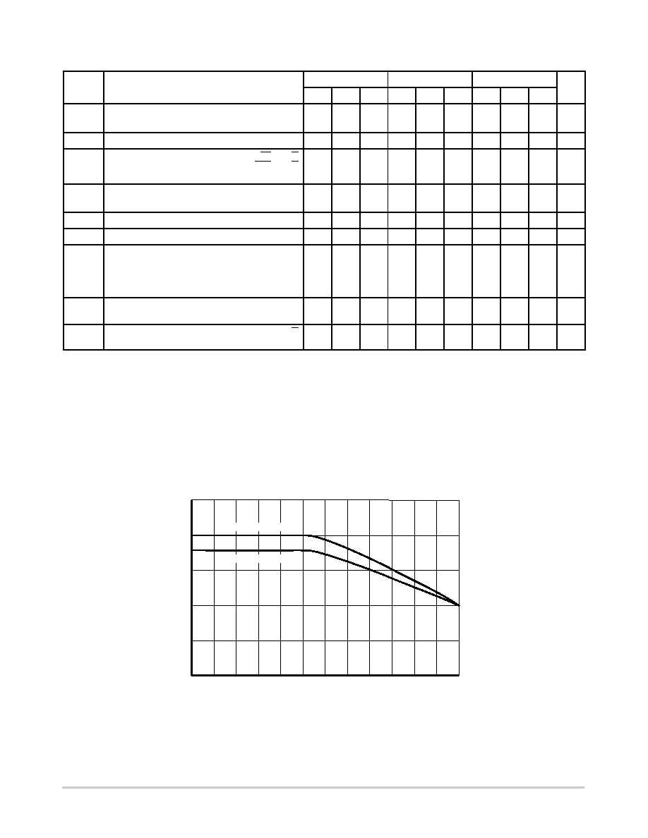
INPUT FREQUENCY (GHz)
Figure 7. Output Voltage Amplitude (VOUTPP) versus
Input Clock Frequency (fin) at Ambient Temperature (Typical)
OUTPUT
VOL
TAGE
AMPLITUDE
(mV)
500
400
300
200
100
0
12
11
10
9
8
7
6
5
4
3
2
1
0
VCC VEE = 3.3 V
VCC VEE = 2.5 V
相关PDF资料 |
PDF描述 |
|---|---|
| TXR40AB45-2012AI | ADPTR TINEL LOCK ANG SHELL 21, G |
| MC14572UBD | IC GATE HEX NAND/NOR/INV 16-SOIC |
| TXR54AB90-2012BI | ADPTR TINEL LOCK ANG SHELL 20,37 |
| TXR40AB90-2014BI | ADPTR TINEL LOCK ANG SHELL 21, G |
| TXR41AB90-2014BI | ADPTR TINEL LOCK ANG SHELL 20,21 |
相关代理商/技术参数 |
参数描述 |
|---|---|
| NB7L86MMNEVB | 功能描述:BOARD EVAL BBG NB7L86MMN RoHS:是 类别:编程器,开发系统 >> 评估演示板和套件 系列:* 标准包装:1 系列:PCI Express® (PCIe) 主要目的:接口,收发器,PCI Express 嵌入式:- 已用 IC / 零件:DS80PCI800 主要属性:- 次要属性:- 已供物品:板 |
| NB7L86MMNG | 功能描述:逻辑门 2.5V/3.3V Diff Clock Data Smart Gate RoHS:否 制造商:Texas Instruments 产品:OR 逻辑系列:LVC 栅极数量:2 线路数量(输入/输出):2 / 1 高电平输出电流:- 16 mA 低电平输出电流:16 mA 传播延迟时间:3.8 ns 电源电压-最大:5.5 V 电源电压-最小:1.65 V 最大工作温度:+ 125 C 安装风格:SMD/SMT 封装 / 箱体:DCU-8 封装:Reel |
| NB7L86MMNR2 | 功能描述:逻辑门 2.5V/3.3V Diff Clock RoHS:否 制造商:Texas Instruments 产品:OR 逻辑系列:LVC 栅极数量:2 线路数量(输入/输出):2 / 1 高电平输出电流:- 16 mA 低电平输出电流:16 mA 传播延迟时间:3.8 ns 电源电压-最大:5.5 V 电源电压-最小:1.65 V 最大工作温度:+ 125 C 安装风格:SMD/SMT 封装 / 箱体:DCU-8 封装:Reel |
| NB7L86MMNR2G | 功能描述:逻辑门 2.5V/3.3V Diff Clock Data Smart Gate RoHS:否 制造商:Texas Instruments 产品:OR 逻辑系列:LVC 栅极数量:2 线路数量(输入/输出):2 / 1 高电平输出电流:- 16 mA 低电平输出电流:16 mA 传播延迟时间:3.8 ns 电源电压-最大:5.5 V 电源电压-最小:1.65 V 最大工作温度:+ 125 C 安装风格:SMD/SMT 封装 / 箱体:DCU-8 封装:Reel |
| NB7LQ572 | 制造商:ONSEMI 制造商全称:ON Semiconductor 功能描述:2.5V / 3.3V Differential 4:1 Mux w/Input Equalizer to 1:2 LVPECL Clock/Data Fanout / Translator |
发布紧急采购,3分钟左右您将得到回复。