参数资料
| 型号: | NB7V52MMNG |
| 厂商: | ON Semiconductor |
| 文件页数: | 1/10页 |
| 文件大小: | 0K |
| 描述: | IC FLIP FLOP DIFF RST/CML 16-QFN |
| 标准包装: | 123 |
| 功能: | 复位 |
| 类型: | D 型 |
| 输出类型: | 差分 |
| 元件数: | 1 |
| 每个元件的位元数: | 1 |
| 延迟时间 - 传输: | 300ps |
| 触发器类型: | 负边沿 |
| 工作温度: | -40°C ~ 85°C |
| 安装类型: | 表面贴装 |
| 封装/外壳: | 16-VFQFN 裸露焊盘 |
| 包装: | 管件 |
Semiconductor Components Industries, LLC, 2009
September, 2009 Rev. 3
1
Publication Order Number:
NB7V52M/D
NB7V52M
1.8V / 2.5V Differential D
Flip-Flop w/ Reset and CML
Outputs
MultiLevel Inputs w/ Internal Termination
Description
The NB7V52M is a 10 GHz differential D flipflop with a
differential asynchronous Reset. The differential D/D, CLK/CLK and
R/R inputs incorporate dual internal 50
W termination resistors and
will accept LVPECL, CML, LVDS logic levels.
When Clock transitions from logic Low to High, Data will be
transferred to the differential CML outputs. The differential Clock
inputs allow the NB7V52M to also be used as a negative edge
triggered device.
The 16 mA differential CML outputs provide matching internal
50
W termination and produce 400 mV output swings when externally
receiver terminated with a 50
W resistor to VCC.
The NB7V52M is offered in a low profile 3 mm x 3 mm 16pin
QFN package. The NB7V52M is a member of the GigaComm
family of high performance clock products. Application notes,
model s, and support document at i o n are avai l a bl e at
www.onsemi.com.
Features
Maximum Input Clock Frequency > 10 GHz
Maximum Input Data Rate > 10 Gb/s
Random Clock Jitter < 0.8 ps RMS, Max
200 ps Typical Propagation Delay
35 ps Typical Rise and Fall Times
Differential CML Outputs, 400 mV PeaktoPeak, Typical
Operating Range: VCC = 1.71 V to 2.625 V with VEE = 0 V
Internal 50 W Input Termination Resistors
QFN16 Package, 3mm x 3mm
40°C to +85°C Ambient Operating Temperature
These are PbFree Devices
A
= Assembly Location
L
= Wafer Lot
Y
= Year
W
= Work Week
G
= PbFree Package
(Note: Microdot may be in either location)
*For additional marking information, refer to
Application Note AND8002/D.
MARKING
DIAGRAM*
QFN16
MN SUFFIX
CASE 485G
http://onsemi.com
See detailed ordering and shipping information in the package
dimensions section on page 9 of this data sheet.
ORDERING INFORMATION
1
NB7V
52M
ALYWG
G
16
1
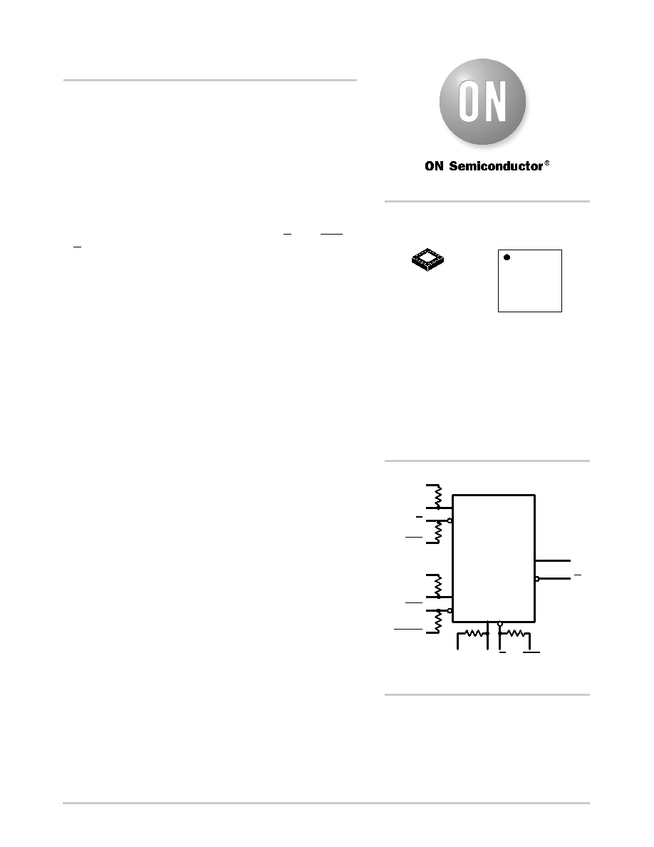
Figure 1. Logic Diagram
Q
RESET
D FlipFlop
CLK
VTCLK
D
VTD
R
D
VTD
CLK
VTCLK
R
VTR
相关PDF资料 |
PDF描述 |
|---|---|
| RTD-2424-R | CONV DC/DC 2W 24VIN +/-24VOUT |
| 74AHC1G07GW,125 | IC BUFF N-INV OP/DRAIN 5TSSOP |
| MC10EP29MNTXG | IC FLIP FLOP DATA/CLK D 20-QFN |
| RTD-2424/P-R | CONV DC/DC 2W 24VIN +/-24VOUT |
| MC100EP29MNTXG | IC FLIP FLOP DATA/CLK D 20-QFN |
相关代理商/技术参数 |
参数描述 |
|---|---|
| NB7V52MMNHTBG | 功能描述:触发器 TSMCD FLIP-FLOP RoHS:否 制造商:Texas Instruments 电路数量:2 逻辑系列:SN74 逻辑类型:D-Type Flip-Flop 极性:Inverting, Non-Inverting 输入类型:CMOS 输出类型: 传播延迟时间:4.4 ns 高电平输出电流:- 16 mA 低电平输出电流:16 mA 电源电压-最大:5.5 V 最大工作温度:+ 85 C 安装风格:SMD/SMT 封装 / 箱体:X2SON-8 封装:Reel |
| NB7V52MMNTXG | 功能描述:触发器 TSMCD FLIP-FLOP RoHS:否 制造商:Texas Instruments 电路数量:2 逻辑系列:SN74 逻辑类型:D-Type Flip-Flop 极性:Inverting, Non-Inverting 输入类型:CMOS 输出类型: 传播延迟时间:4.4 ns 高电平输出电流:- 16 mA 低电平输出电流:16 mA 电源电压-最大:5.5 V 最大工作温度:+ 85 C 安装风格:SMD/SMT 封装 / 箱体:X2SON-8 封装:Reel |
| NB7V585M | 制造商:ONSEMI 制造商全称:ON Semiconductor 功能描述:1.8V / 2.5V Differential 2:1 Mux Input to 1:6 CML Clock/Data Fanout Buffer/Translator |
| NB7V585MMNG | 功能描述:时钟驱动器及分配 TSMCFANOUT BFFR/XLTR RoHS:否 制造商:Micrel 乘法/除法因子:1:4 输出类型:Differential 最大输出频率:4.2 GHz 电源电压-最大: 电源电压-最小:5 V 最大工作温度:+ 85 C 封装 / 箱体:SOIC-8 封装:Reel |
| NB7V585MMNR4G | 功能描述:时钟驱动器及分配 TSMCFANOUT BFFR/XLTR RoHS:否 制造商:Micrel 乘法/除法因子:1:4 输出类型:Differential 最大输出频率:4.2 GHz 电源电压-最大: 电源电压-最小:5 V 最大工作温度:+ 85 C 封装 / 箱体:SOIC-8 封装:Reel |
发布紧急采购,3分钟左右您将得到回复。