参数资料
| 型号: | NB7V52MMNTXG |
| 厂商: | ON Semiconductor |
| 文件页数: | 3/10页 |
| 文件大小: | 0K |
| 描述: | IC FLIP FLOP DIFF RST/CML 16-QFN |
| 标准包装: | 3,000 |
| 功能: | 复位 |
| 类型: | D 型 |
| 输出类型: | 差分 |
| 元件数: | 1 |
| 每个元件的位元数: | 1 |
| 延迟时间 - 传输: | 300ps |
| 触发器类型: | 负边沿 |
| 工作温度: | -40°C ~ 85°C |
| 安装类型: | 表面贴装 |
| 封装/外壳: | 16-VFQFN 裸露焊盘 |
| 包装: | 带卷 (TR) |
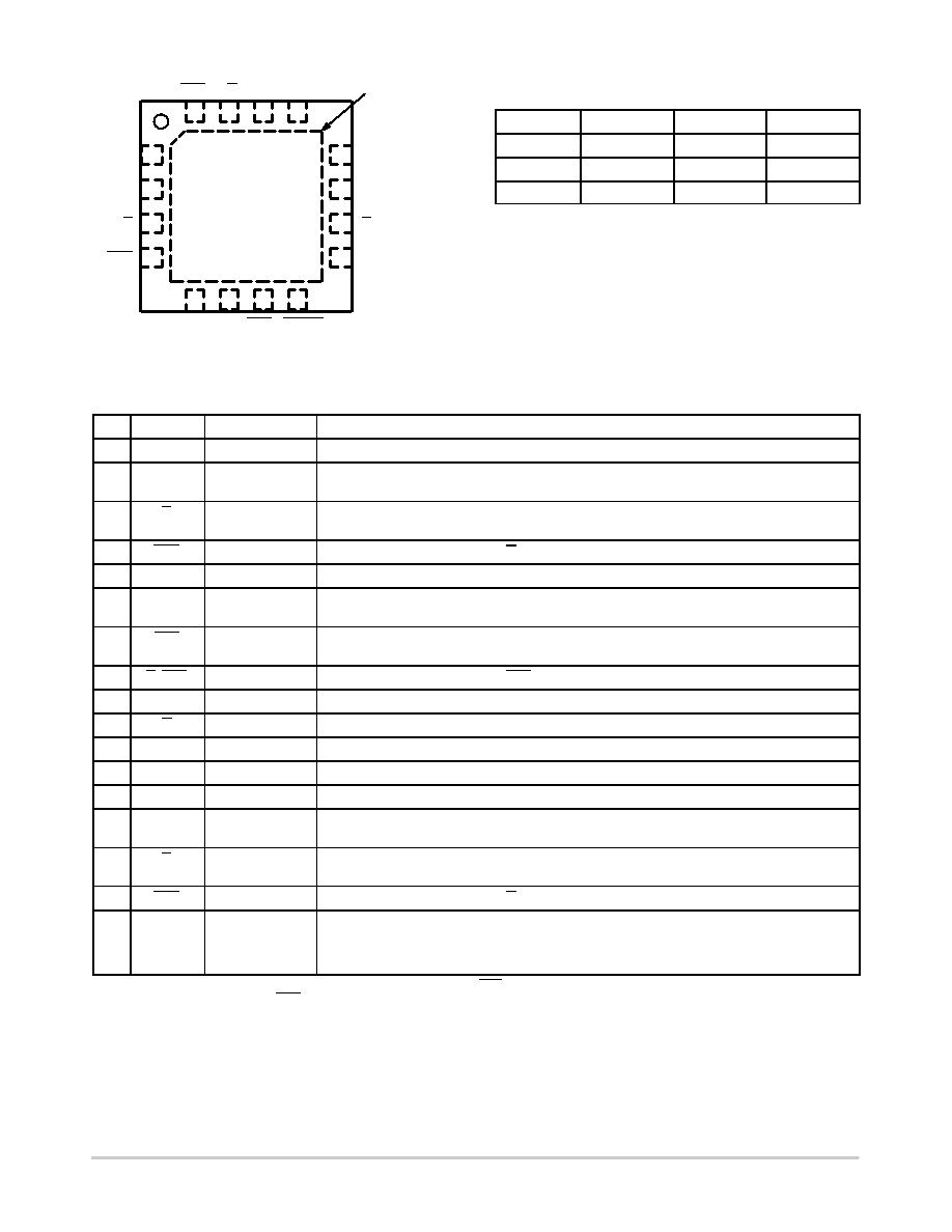
NB7V52M
http://onsemi.com
2
VTCLK CLK CLK VTCLK
VTR
R
VTR
VCC
Q
VEE
VTD
D
VTD
5
678
16
15
14
13
12
11
10
9
1
2
3
4
NB7V52M
Exposed Pad (EP)
Figure 2. Pin Configuration (Top View)
Table 1. INPUT/OUTPUT SELECT TRUTH TABLE
R
D
CLK
Q
H
x
L
Z
L
H
Z
H
Z = LOW to HIGH Transition
x = Don’t care
Table 1. Pin Description
Pin
Name
I/O
Description
1
VTD
Internal 50 W Termination Pin for D
2
D
LVPECL, CML,
LVDS Input
Noninverted Differential Data Input. (Note 1)
3
D
LVPECL, CML,
LVDS Input
Inverted Differential Data Input. (Note 1)
4
VTD
Internal 50 W Termination Pin for D
5
VTCLK
Internal 50 W Termination Pin for CLK
6
CLK
LVPECL, CML,
LVDS Input
Noninverted Differential Clock Input. (Note 1)
7
CLK
LVPECL, CML,
LVDS Input
Inverted Differential Clock Input. (Note 1)
8
VTCLK
Internal 50 W Termination Pin for CLK
9
VEE
Negative Supply Voltage. (Note 2)
10
Q
CML Output
Inverted Differential Output
11
Q
CML Output
Noninverted Differential Output
12
VCC
Positive Supply Voltage. (Note 2)
13
VTR
Internal 50 W Termination Pin for R
14
R
LVPECL, CML,
LVDS Input
Noninverted Asynchronous Differential Reset Input. (Note 1)
15
R
LVPECL, CML,
LVDS Input
Inverted Asynchronous Differential Reset Input. (Note 1)
16
VTR
Internal 50 W Termination Pin for R
EP
The Exposed Pad (EP) on the QFN16 package bottom is thermally connected to the die for
improved heat transfer out of package. The exposed pad must be attached to a heatsinking
conduit. The pad is not electrically connected to the die, but is recommended to be electrically
and thermally connected to VEE on the PC board.
1. In the differential configuration when the input termination pins (VTx, VTx) are connected to a common termination voltage or left open, and
if no signal is applied on CLK/CLK input, then the device will be susceptible to selfoscillation.
2. All VCC and GND pins must be externally connected to a power supply for proper operation.
相关PDF资料 |
PDF描述 |
|---|---|
| MC10E151FNR2G | IC REGISTER 6BIT D ECL 5V 28PLCC |
| M83723/82W1415NLC | CONN HSG RCPT 15POS WALL MT SCKT |
| MS3451L22-2B | CONN HSG RCPT 3POS CBL MNT SCKT |
| 6102311 | CONN TERM BLK SCRWLESS BLUE 5MM |
| MS27473T24B24SALC | CONN HSG PLUG 24POS STRGHT SCKT |
相关代理商/技术参数 |
参数描述 |
|---|---|
| NB7V585M | 制造商:ONSEMI 制造商全称:ON Semiconductor 功能描述:1.8V / 2.5V Differential 2:1 Mux Input to 1:6 CML Clock/Data Fanout Buffer/Translator |
| NB7V585MMNG | 功能描述:时钟驱动器及分配 TSMCFANOUT BFFR/XLTR RoHS:否 制造商:Micrel 乘法/除法因子:1:4 输出类型:Differential 最大输出频率:4.2 GHz 电源电压-最大: 电源电压-最小:5 V 最大工作温度:+ 85 C 封装 / 箱体:SOIC-8 封装:Reel |
| NB7V585MMNR4G | 功能描述:时钟驱动器及分配 TSMCFANOUT BFFR/XLTR RoHS:否 制造商:Micrel 乘法/除法因子:1:4 输出类型:Differential 最大输出频率:4.2 GHz 电源电压-最大: 电源电压-最小:5 V 最大工作温度:+ 85 C 封装 / 箱体:SOIC-8 封装:Reel |
| NB7V586M | 制造商:ONSEMI 制造商全称:ON Semiconductor 功能描述:1.8V Differential 2:1 Mux Input to 1.2V/1.8V 1:6 CML Clock/Data Fanout Buffer / Translator |
| NB7V586MMNG | 功能描述:时钟驱动器及分配 TSMCFANOUT BFFR/XLTR RoHS:否 制造商:Micrel 乘法/除法因子:1:4 输出类型:Differential 最大输出频率:4.2 GHz 电源电压-最大: 电源电压-最小:5 V 最大工作温度:+ 85 C 封装 / 箱体:SOIC-8 封装:Reel |
发布紧急采购,3分钟左右您将得到回复。