参数资料
| 型号: | NBSG16MMNG |
| 厂商: | ON Semiconductor |
| 文件页数: | 1/11页 |
| 文件大小: | 0K |
| 描述: | IC RCVR/DVR RSECL SIGE DF 16QFN |
| 标准包装: | 123 |
| 类型: | 收发器 |
| 应用: | 仪表 |
| 安装类型: | 表面贴装 |
| 封装/外壳: | 16-VFQFN 裸露焊盘 |
| 供应商设备封装: | 16-QFN(3x3) |
| 包装: | 管件 |
| 其它名称: | NBSG16MMNGOS |
Semiconductor Components Industries, LLC, 2009
March, 2009 Rev. 7
1
Publication Order Number:
NBSG16M/D
NBSG16M
2.5 V/3.3 VMultilevel Input
to CML Clock/Data
Receiver/Driver/Translator
Buffer
Description
The NBSG16M is a differential current mode logic (CML)
receiver/driver/translator buffer. The device is functionally equivalent
to the EP16, LVEP16, or SG16 devices with CML output structure and
lower EMI capabilities.
Inputs incorporate internal 50
W termination resistors and accept
LVNECL (Negative ECL), LVPECL (Positive ECL), LVTTL,
LVCMOS, CML, or LVDS. The CML output structure contains
internal 50
W source termination resistor to VCC. The device
generates 400 mV output amplitude with 50
W receiver resistor to
VCC.
The VBB pin is internally generated voltage supply available to this
device only. For all singleended input conditions, the unused
complementary differential input is connected to VBB as a switching
reference voltage. VBB may also rebias AC coupled inputs. When
used, decouple VBB via a 0.01 mF capacitor and limit current sourcing
or sinking to 0.5 mA. When not used, VBB output should be left open.
Features
Maximum Input Clock Frequency > 10 GHz Typical
Maximum Input Data Rate > 10 Gb/s Typical
120 ps Typical Propagation Delay
35 ps Typical Rise and Fall Times
Positive CML Output with Operating Range:
VCC = 2.375 V to 3.465 V with VEE = 0 V
Negative CML Output with RSNECL or NECL Inputs with
Operating Range: VCC = 0 V with VEE = 2.375 V to 3.465 V
CML Output Level; 400 mV PeaktoPeak Output with
50
W Receiver Resistor to VCC
50 W Internal Input and Output Termination Resistors
Compatible with Existing 2.5 V/3.3 V LVEP, EP, LVEL
and SG Devices
VBB Reference Voltage Output
PbFree Packages are Available
*For additional marking information, refer to
Application Note AND8002/D.
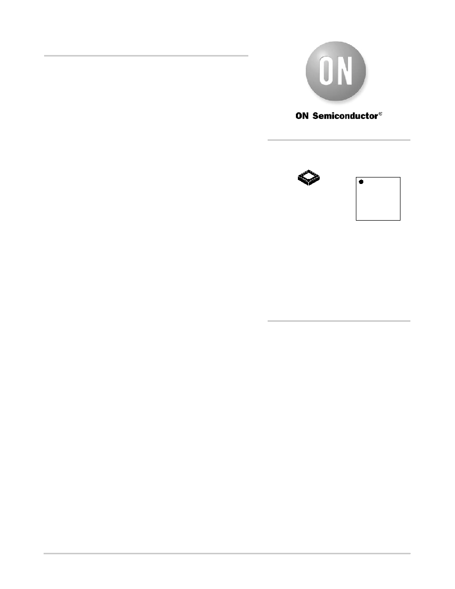
MARKING
DIAGRAM*
http://onsemi.com
QFN16
MN SUFFIX
CASE 485G
1
A
= Assembly Location
L
= Wafer Lot
Y
= Year
W
= Work Week
G
= PbFree Package
See detailed ordering and shipping information in the package
dimensions section on page 10 of this data sheet.
ORDERING INFORMATION
(Note: Microdot may be in either location)
16
SG
16M
ALYW G
G
1
相关PDF资料 |
PDF描述 |
|---|---|
| LFXP3E-5T100C | IC FPGA 3.1KLUTS 62I/O 100-TQFP |
| LFXP3E-5TN100C | IC FPGA 3.1KLUTS 62I/O 100-TQFP |
| LFXP3E-4TN100I | IC FPGA 3.1KLUTS 62I/O 100-TQFP |
| LFXP3E-4T100I | IC FPGA 3.1KLUTS 62I/O 100-TQFP |
| LFXP3C-5TN100C | IC FPGA 3.1KLUTS 62I/O 100-TQFP |
相关代理商/技术参数 |
参数描述 |
|---|---|
| NBSG16MMNR2 | 功能描述:缓冲器和线路驱动器 2.5V/3.3V Multilevel RoHS:否 制造商:Micrel 输入线路数量:1 输出线路数量:2 极性:Non-Inverting 电源电压-最大:+/- 5.5 V 电源电压-最小:+/- 2.37 V 最大工作温度:+ 85 C 安装风格:SMD/SMT 封装 / 箱体:MSOP-8 封装:Reel |
| NBSG16MMNR2G | 功能描述:缓冲器和线路驱动器 2.5V/3.3V Multilevel Input Clk/Data RCVR RoHS:否 制造商:Micrel 输入线路数量:1 输出线路数量:2 极性:Non-Inverting 电源电压-最大:+/- 5.5 V 电源电压-最小:+/- 2.37 V 最大工作温度:+ 85 C 安装风格:SMD/SMT 封装 / 箱体:MSOP-8 封装:Reel |
| NBSG16MN | 功能描述:缓冲器和线路驱动器 2.5V/3.3V SiGe Diff RoHS:否 制造商:Micrel 输入线路数量:1 输出线路数量:2 极性:Non-Inverting 电源电压-最大:+/- 5.5 V 电源电压-最小:+/- 2.37 V 最大工作温度:+ 85 C 安装风格:SMD/SMT 封装 / 箱体:MSOP-8 封装:Reel |
| NBSG16MNG | 功能描述:缓冲器和线路驱动器 2.5V/3.3V SiGe Diff Receiver w/RSECL RoHS:否 制造商:Micrel 输入线路数量:1 输出线路数量:2 极性:Non-Inverting 电源电压-最大:+/- 5.5 V 电源电压-最小:+/- 2.37 V 最大工作温度:+ 85 C 安装风格:SMD/SMT 封装 / 箱体:MSOP-8 封装:Reel |
| NBSG16MNHTBG | 功能描述:缓冲器和线路驱动器 2.5/3.3V SIGE DF/RCV BBG RoHS:否 制造商:Micrel 输入线路数量:1 输出线路数量:2 极性:Non-Inverting 电源电压-最大:+/- 5.5 V 电源电压-最小:+/- 2.37 V 最大工作温度:+ 85 C 安装风格:SMD/SMT 封装 / 箱体:MSOP-8 封装:Reel |
发布紧急采购,3分钟左右您将得到回复。