参数资料
| 型号: | NBSG16MMNG |
| 厂商: | ON Semiconductor |
| 文件页数: | 4/11页 |
| 文件大小: | 0K |
| 描述: | IC RCVR/DVR RSECL SIGE DF 16QFN |
| 标准包装: | 123 |
| 类型: | 收发器 |
| 应用: | 仪表 |
| 安装类型: | 表面贴装 |
| 封装/外壳: | 16-VFQFN 裸露焊盘 |
| 供应商设备封装: | 16-QFN(3x3) |
| 包装: | 管件 |
| 其它名称: | NBSG16MMNGOS |
NBSG16M
http://onsemi.com
2
VCC NC VEE VEE
VCC VBB VEE VEE
VCC
Q
VCC
VTD
D
VTD
5
678
16
15
14
13
12
11
10
9
1
2
3
4
NBSG16M
Exposed Pad (EP)
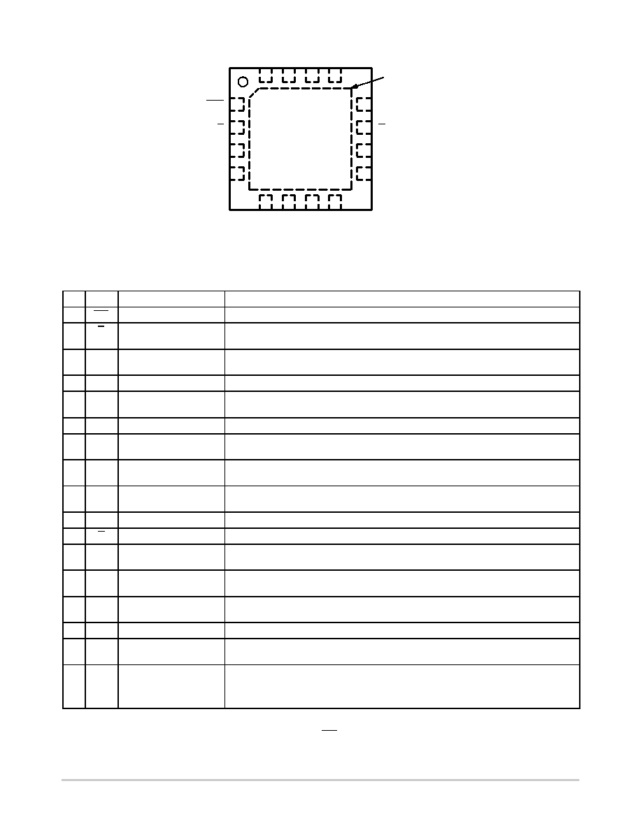
Figure 1. QFN16 Pinout (Top View)
Table 1. PIN DESCRIPTION
Pin
Name
I/O
Description
1
VTD
2
D
LVDS, CML, ECL, LVTTL,
LVCMOS Input
Inverted Differential Input (Note 3)
3
D
LVDS, CML, ECL, LVTTL,
LVCMOS Input
Noninverted Differential Input. (Note 3)
4
VTD
5
VCC
Positive Supply Voltage. All VCC pins must be externally connected to Power Supply to guar-
antee proper operation.
6
NC
No Connect (Note 1)
7
VEE
Negative Supply Voltage. All VEE pins must be externally connected to Power Supply to guar-
antee proper operation.
8
VEE
Negative Supply Voltage. All VEE pins must be externally connected to Power Supply to guar-
antee proper operation.
9
VCC
Positive Supply Voltage. All VCC pins must be externally connected to Power Supply to guar-
antee proper operation.
10
Q
CML Output
Noninverted CML Differential Output with Internal 50 W Source Termination Resistor. (Note 2)
11
Q
CML Output
Inverted CML Differential Output with Internal 50 W Source Termination Resistor. (Note 2)
12
VCC
Positive Supply Voltage. All VCC pins must be externally connected to Power Supply to guar-
antee proper operation.
13
VEE
Negative Supply Voltage. All VEE pins must be externally connected to Power Supply to guar-
antee proper operation.
14
VEE
Negative Supply Voltage. All VEE pins must be externally connected to Power Supply to guar-
antee proper operation.
15
VBB
Internally Generated ECL Reference Output Voltage
16
VCC
Positive Supply Voltage. All VCC pins must be externally connected to Power Supply to guar-
antee proper operation.
EP
The Exposed Pad (EP) and the QFN16 package bottom is thermally connected to the die
for improved heat transfer out of package. The exposed pad must be attached to a heat
sinking conduit. The pad is not electrically connected to the die but may be electrically and
thermally connected to VEE on the PC board.
1. The NC pins are electrically connected to the die and MUST be left open.
2. CML outputs require 50 W receiver termination resistor to VCC for proper operation.
3. In the differential configuration when the input termination pin (VTD, VTD) are connected to a common termination voltage, and if no signal
is applied then the device will be susceptible to selfoscillation.
相关PDF资料 |
PDF描述 |
|---|---|
| LFXP3E-5T100C | IC FPGA 3.1KLUTS 62I/O 100-TQFP |
| LFXP3E-5TN100C | IC FPGA 3.1KLUTS 62I/O 100-TQFP |
| LFXP3E-4TN100I | IC FPGA 3.1KLUTS 62I/O 100-TQFP |
| LFXP3E-4T100I | IC FPGA 3.1KLUTS 62I/O 100-TQFP |
| LFXP3C-5TN100C | IC FPGA 3.1KLUTS 62I/O 100-TQFP |
相关代理商/技术参数 |
参数描述 |
|---|---|
| NBSG16MMNR2 | 功能描述:缓冲器和线路驱动器 2.5V/3.3V Multilevel RoHS:否 制造商:Micrel 输入线路数量:1 输出线路数量:2 极性:Non-Inverting 电源电压-最大:+/- 5.5 V 电源电压-最小:+/- 2.37 V 最大工作温度:+ 85 C 安装风格:SMD/SMT 封装 / 箱体:MSOP-8 封装:Reel |
| NBSG16MMNR2G | 功能描述:缓冲器和线路驱动器 2.5V/3.3V Multilevel Input Clk/Data RCVR RoHS:否 制造商:Micrel 输入线路数量:1 输出线路数量:2 极性:Non-Inverting 电源电压-最大:+/- 5.5 V 电源电压-最小:+/- 2.37 V 最大工作温度:+ 85 C 安装风格:SMD/SMT 封装 / 箱体:MSOP-8 封装:Reel |
| NBSG16MN | 功能描述:缓冲器和线路驱动器 2.5V/3.3V SiGe Diff RoHS:否 制造商:Micrel 输入线路数量:1 输出线路数量:2 极性:Non-Inverting 电源电压-最大:+/- 5.5 V 电源电压-最小:+/- 2.37 V 最大工作温度:+ 85 C 安装风格:SMD/SMT 封装 / 箱体:MSOP-8 封装:Reel |
| NBSG16MNG | 功能描述:缓冲器和线路驱动器 2.5V/3.3V SiGe Diff Receiver w/RSECL RoHS:否 制造商:Micrel 输入线路数量:1 输出线路数量:2 极性:Non-Inverting 电源电压-最大:+/- 5.5 V 电源电压-最小:+/- 2.37 V 最大工作温度:+ 85 C 安装风格:SMD/SMT 封装 / 箱体:MSOP-8 封装:Reel |
| NBSG16MNHTBG | 功能描述:缓冲器和线路驱动器 2.5/3.3V SIGE DF/RCV BBG RoHS:否 制造商:Micrel 输入线路数量:1 输出线路数量:2 极性:Non-Inverting 电源电压-最大:+/- 5.5 V 电源电压-最小:+/- 2.37 V 最大工作温度:+ 85 C 安装风格:SMD/SMT 封装 / 箱体:MSOP-8 封装:Reel |
发布紧急采购,3分钟左右您将得到回复。