- 您现在的位置:买卖IC网 > PDF目录16315 > NBSG16VSBAEVB (ON Semiconductor)BOARD EVAL BBG NBSG16VSBA PDF资料下载
参数资料
| 型号: | NBSG16VSBAEVB |
| 厂商: | ON Semiconductor |
| 文件页数: | 14/14页 |
| 文件大小: | 0K |
| 描述: | BOARD EVAL BBG NBSG16VSBA |
| 产品变化通告: | Product Discontinuation 21/Jun/2007 |
| 标准包装: | 1 |
| 主要目的: | 接口 |
| 嵌入式: | 否 |
| 已用 IC / 零件: | NBSG16VS |
| 主要属性: | * |
| 次要属性: | * |
| 已供物品: | * |
| 相关产品: | NBSG16VSMNHTBG-ND - IC RCVR/DVR SIGE DIFF 16QFN NBSG16VSMNR2GOS-ND - IC RCVR/DRIVER SIGE DIFF 16QFN NBSG16VSMNGOS-ND - IC RCVR/DRIVER SIGE DIFF 16QFN |
| 其它名称: | NBSG16VSBAEVB-ND NBSG16VSBAEVBOS |
NBSG16VS
http://onsemi.com
9
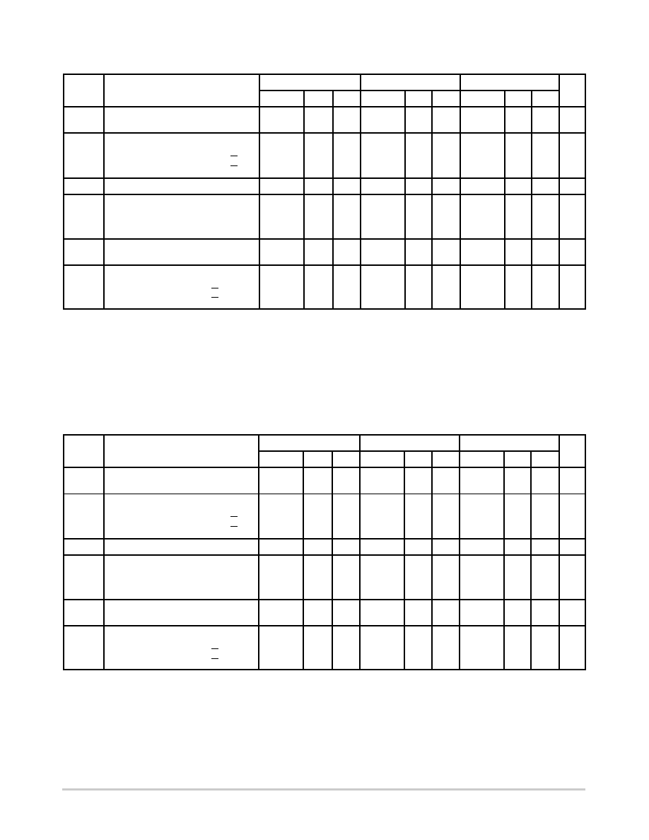
Table 10. AC CHARACTERISTICS for QFN16 VCC = 0 V; VEE = 3.465 V to 3.0 V or VCC = 3.0 V to 3.465 V; VEE = 0 V
Symbol
Characteristic
40°C
25°C
85°C
Unit
Min
Typ
Max
Min
Typ
Max
Min
Typ
Max
fmax
Maximum Frequency
10
(Note 37)
12
10
(Note 37)
12
10
(Note 37)
12
GHz
tPLH,
tPHL
Propagation Delay to
Output Differential
(VCTRL = VCC 2 V) D → Q, Q
(VCTRL = VCC 1 V) D → Q, Q
100
140
135
180
100
140
135
180
100
80
140
135
180
220
ps
tSKEW
Duty Cycle Skew (Note 35)
3
20
3
15
3
10
ps
tJITTER
RMS Random Clock Jitter
fin < 10 GHz
PeaktoPeak Data Dependent Jitter
fin < 10 Gb/s
0.5
TBD
2
0.5
TBD
2
0.5
TBD
2
ps
VINPP
Input Voltage Swing/Sensitivity
(Differential Configuration) (Note 36)
75
2600
75
2600
75
2600
mV
tr
tf
Output Rise/Fall Times (20% 80%)
@ 1 GHz
(VCTRL = VCC 2 V) Q, Q
(VCTRL = VCC 1 V) Q, Q
30
45
40
55
50
30
45
40
55
50
30
45
40
55
50
ps
NOTE: Device will meet the specifications after thermal equilibrium has been established when mounted in a test socket or printed circuit
board with maintained transverse airflow greater than 500 lfpm. Electrical parameters are guaranteed only over the declared
operating temperature range. Functional operation of the device exceeding these conditions is not implied. Device specification limit
values are applied individually under normal operating conditions and not valid simultaneously.
34.Measured using a 500 mV source, 50% duty cycle clock source. All loading with 50 W to VCC2.0 V. Input edge rates 40 ps (20% 80%).
36.VINPP(MAX) cannot exceed VCC VEE (applicable only when VCC VEE t 2600 mV).
37.Conditions include input amplitude of 500 mV and VCTRL = VCC 2 V. Minimum output amplitude guarantee of 100 mV (see Output PP
Spec in Figure 8).
Table 11. AC CHARACTERISTICS for QFN16 VCC = 0 V; 3.0 V tVEE v 2.375 V or 2.375 V v VCC t 3.0 V; VEE = 0 V
Symbol
Characteristic
40°C
25°C
85°C
Unit
Min
Typ
Max
Min
Typ
Max
Min
Typ
Max
fmax
Maximum Frequency
10
(Note 41)
12
10
(Note 41)
12
10
(Note 41)
12
GHz
tPLH,
tPHL
Propagation Delay to
Output Differential
(VCTRL = VCC 2 V) D → Q, Q
(VCTRL = VCC 1 V) D → Q, Q
100
140
135
180
100
140
135
180
80
100
140
135
180
220
ps
tSKEW
Duty Cycle Skew (Note 39)
3
20
3
15
3
10
ps
tJITTER
RMS Random Clock Jitter
fin < 10 GHz
PeaktoPeak Data Dependent Jitter
fin < 10 Gb/s
0.5
TBD
3
0.5
TBD
3
0.5
TBD
3
ps
VINPP
Input Voltage Swing/Sensitivity
(Differential Configuration) (Note 40)
75
2600
75
2600
75
2600
mV
tr
tf
Output Rise/Fall Times (20% 80%)
@ 1 GHz
(VCTRL = VCC 2 V) Q, Q
(VCTRL = VCC 1 V) Q, Q
25
22
50
45
70
60
25
22
50
45
70
60
25
22
50
45
70
60
ps
NOTE: Device will meet the specifications after thermal equilibrium has been established when mounted in a test socket or printed circuit
board with maintained transverse airflow greater than 500 lfpm. Electrical parameters are guaranteed only over the declared
operating temperature range. Functional operation of the device exceeding these conditions is not implied. Device specification limit
values are applied individually under normal operating conditions and not valid simultaneously.
38.Measured using a 500 mV source, 50% duty cycle clock source. All loading with 50 W to VCC2.0 V. Input edge rates 40 ps (20% 80%).
40.VINPP(MAX) cannot exceed VCC VEE (applicable only when VCC VEE t 2600 mV).
41.Conditions include input amplitude of 500 mV and VCTRL = VCC 2 V. Minimum output amplitude guarantee of 100 mV (see Output PP
Spec in Figure 9).
相关PDF资料 |
PDF描述 |
|---|---|
| ECO-S2DB102CA | CAP ALUM 1000UF 200V 20% SNAP |
| 3-6828151-0 | C/A,2.0MM,RIS,XG,50/125,SC DUP |
| 2-6278893-5 | C/A 62.5/125UM LSZH MTRJ 4M1 |
| ECO-S1EA183EA | CAP ALUM 18000UF 25V 20% SNAP |
| ECO-S1JA562DA | CAP ALUM 5600UF 63V 20% SNAP |
相关代理商/技术参数 |
参数描述 |
|---|---|
| NBSG16VSBAHTBG | 功能描述:缓冲器和线路驱动器 BBG 2.5V/3.3V SIGE DIFF RoHS:否 制造商:Micrel 输入线路数量:1 输出线路数量:2 极性:Non-Inverting 电源电压-最大:+/- 5.5 V 电源电压-最小:+/- 2.37 V 最大工作温度:+ 85 C 安装风格:SMD/SMT 封装 / 箱体:MSOP-8 封装:Reel |
| NBSG16VSBAR2 | 功能描述:缓冲器和线路驱动器 2.5V/3.3V SiGe Diff RoHS:否 制造商:Micrel 输入线路数量:1 输出线路数量:2 极性:Non-Inverting 电源电压-最大:+/- 5.5 V 电源电压-最小:+/- 2.37 V 最大工作温度:+ 85 C 安装风格:SMD/SMT 封装 / 箱体:MSOP-8 封装:Reel |
| NBSG16VSMAG | 功能描述:IC RCVR/DRVR SIGE DIFF 16-FCLGA RoHS:是 类别:集成电路 (IC) >> 专用 IC 系列:- 产品培训模块:Lead (SnPb) Finish for COTS Obsolescence Mitigation Program 标准包装:1 系列:- 类型:调帧器 应用:数据传输 安装类型:表面贴装 封装/外壳:400-BBGA 供应商设备封装:400-PBGA(27x27) 包装:散装 |
| NBSG16VSMN | 功能描述:缓冲器和线路驱动器 2.5V/3.3V SiGe Diff RoHS:否 制造商:Micrel 输入线路数量:1 输出线路数量:2 极性:Non-Inverting 电源电压-最大:+/- 5.5 V 电源电压-最小:+/- 2.37 V 最大工作温度:+ 85 C 安装风格:SMD/SMT 封装 / 箱体:MSOP-8 封装:Reel |
| NBSG16VSMNG | 功能描述:缓冲器和线路驱动器 2.5V/3.3V SiGe Diff w/Variable Output RoHS:否 制造商:Micrel 输入线路数量:1 输出线路数量:2 极性:Non-Inverting 电源电压-最大:+/- 5.5 V 电源电压-最小:+/- 2.37 V 最大工作温度:+ 85 C 安装风格:SMD/SMT 封装 / 箱体:MSOP-8 封装:Reel |
发布紧急采购,3分钟左右您将得到回复。