- 您现在的位置:买卖IC网 > PDF目录15768 > NBSG53ABAEVB (ON Semiconductor)BOARD EVAL BBG NBSG53ABA PDF资料下载
参数资料
| 型号: | NBSG53ABAEVB |
| 厂商: | ON Semiconductor |
| 文件页数: | 11/18页 |
| 文件大小: | 0K |
| 描述: | BOARD EVAL BBG NBSG53ABA |
| 产品变化通告: | Product Discontinuation 21/Jun/2007 |
| 标准包装: | 1 |
| 其它名称: | NBSG53ABAEVB-ND NBSG53ABAEVBOS |
NBSG53A
http://onsemi.com
2
VTD
CLK
VTCLK
VCC
R
VTCLK
D
VTD
VCC
VEE
SEL
OLS
Q
A
B
C
D
12
3
4
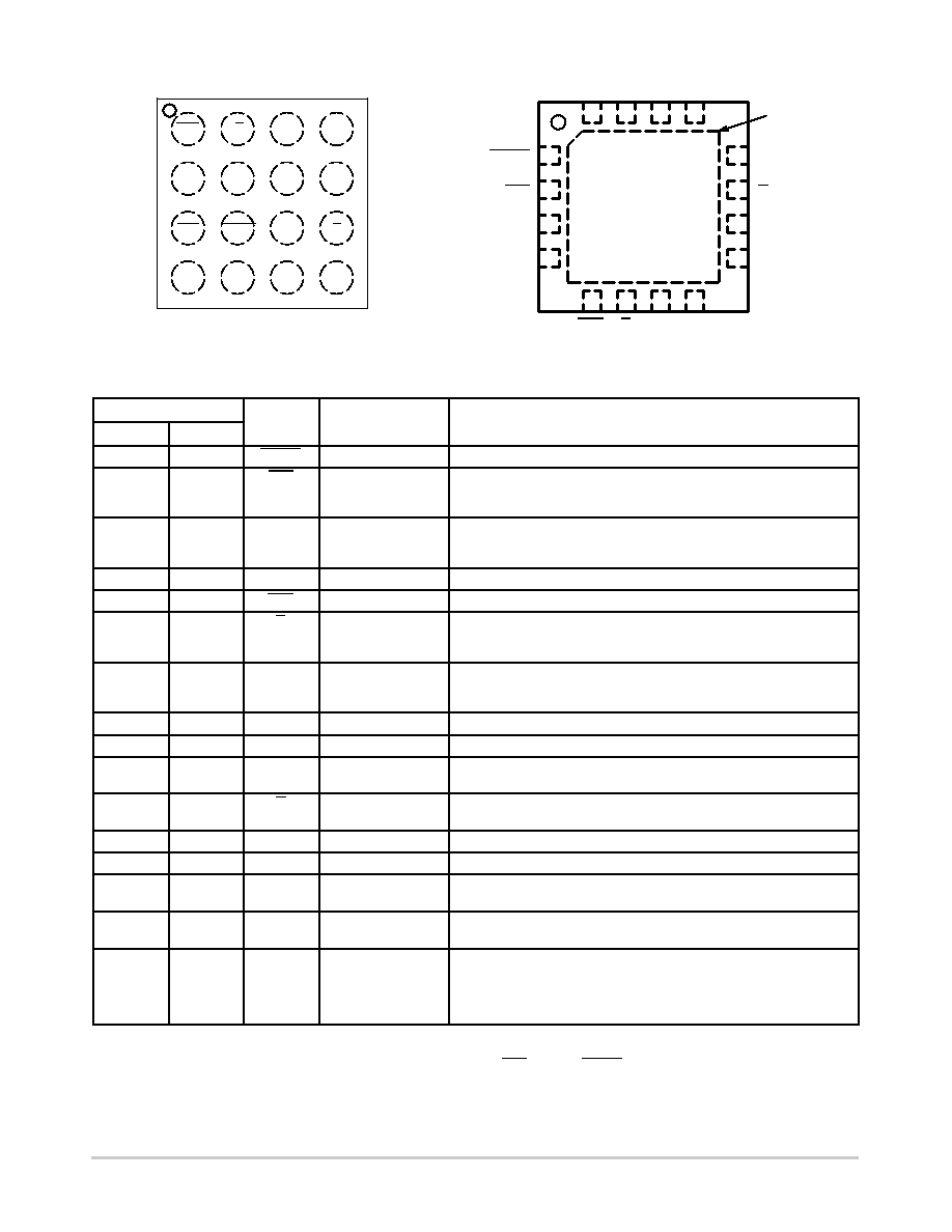
Figure 1. BGA16 Pinout (Top View)
VTD
D
VTD
VCC
R
SEL OLS
VEE
Q
VCC
VTCLK
CLK
VTCLK
56
7
8
16
15
14
13
12
11
10
9
1
2
3
4
NBSG53A
Exposed Pad
(EP)
Figure 2. QFN16 Pinout (Top View)
Table 1. PIN DESCRIPTION
Pin
Name
I/O
Description
BGA
QFN
C2
1
VTCLK
Internal 50 W Termination Pin. See Table 4.
C1
2
CLK
ECL, CML,
LVCMOS, LVDS,
LVTTL Input
Inverted Differential Input.
B1
3
CLK
ECL, CML,
LVCMOS, LVDS,
LVTTL Input
Noninverted Differential Input.
B2
4
VTCLK
Internal 50 W Termination Pin. See Table 4.
A1
5
VTD
Internal 50 W termination pin. See Table 4.
A2
6
D
ECL, CML,
LVCMOS, LVDS,
LVTTL Input
Inverted Differential Input.
A3
7
D
ECL, CML,
LVCMOS, LVDS,
LVTTL Input
Noninverted Differential Input.
A4
8
VTD
Internal 50 W Termination Pin. See Table 4.
D1,B3
9,16
VCC
Positive Supply Voltage
B4
10
Q
RSECL Output
NonInverted Differential Output. Typically Terminated with 50 W Resistor
to VTT = VCC 2 V.
C4
11
Q
RSECL Output
Inverted Differential Output. Typically Terminated with 50 W Resistor to
VTT = VCC 2 V.
C3
12
VEE
Negative Supply Voltage
D4
13
OLS*
Input
Input Pin for the Output Level Select (OLS). See Table 2.
D3
14
SEL
LVECL, LVCMOS,
LVTTL Input
Select Logic Input. Internal 75 kW to VEE.
D2
15
R
LVECL, LVCMOS,
LVTTL Input
Reset D FlipFlop. Internal 75 kW to VEE.
N/A
EP
The Exposed Pad (EP) and the QFN16 package bottom is thermally
connected to the die for improved heat transfer out of package. The
exposed pad must be attached to a heatsinking conduit. The pad is not
electrically connected to the die but may be electrically and thermally
connected to VEE on the PC board.
1. All VCC and VEE pins must be externally connected to Power Supply to guarantee proper operation. The thermally exposed pad (EP) on
package bottom (see case drawing) must be attached to a heatsinking conduit.
2. In the differential configuration when the input termination pins (VTD, VTD, VTCLK, VTCLK) are connected to a common termination
voltage, and if no signal is applied then the device will be susceptible to selfoscillation.
3. When an output level of 400 mV is desired and VCC VEE > 3.0 V, 2KW resistor should be connected from OLS pin to VEE.
相关PDF资料 |
PDF描述 |
|---|---|
| NBSG16BAEVB | BOARD EVALUATION BBG NBSG16BA |
| 1300060241 | CORDSET FEMALE 20' 16/3 PVC |
| 1300100221 | CORDSET MALE-FEMALE 6' 16/3 PVC |
| MPC8360E-MDS-PBE | BOARD PROCESSOR FOR MPC8360E |
| VI-B5P-EY-F3 | CONVERTER MOD DC/DC 13.8V 50W |
相关代理商/技术参数 |
参数描述 |
|---|---|
| NBSG53ABAHTBG | 功能描述:时钟驱动器及分配 2.5/3.3V SEL DIFF CLK RoHS:否 制造商:Micrel 乘法/除法因子:1:4 输出类型:Differential 最大输出频率:4.2 GHz 电源电压-最大: 电源电压-最小:5 V 最大工作温度:+ 85 C 封装 / 箱体:SOIC-8 封装:Reel |
| NBSG53ABAR2 | 功能描述:触发器 2.5V/3.3V SiGe Diff RoHS:否 制造商:Texas Instruments 电路数量:2 逻辑系列:SN74 逻辑类型:D-Type Flip-Flop 极性:Inverting, Non-Inverting 输入类型:CMOS 输出类型: 传播延迟时间:4.4 ns 高电平输出电流:- 16 mA 低电平输出电流:16 mA 电源电压-最大:5.5 V 最大工作温度:+ 85 C 安装风格:SMD/SMT 封装 / 箱体:X2SON-8 封装:Reel |
| NBSG53AMA1TBG | 制造商:ON Semiconductor 功能描述:SIGE DIF CLK DATA D F-F - Tape and Reel |
| NBSG53AMAG | 功能描述:IC FLIP FLOP/CLK DIVIDER 16FCLGA RoHS:是 类别:集成电路 (IC) >> 逻辑 - 触发器 系列:- 产品变化通告:Product Discontinuation 27/Jan/2012 标准包装:2,000 系列:74LCX 功能:标准 类型:D 型总线 输出类型:三态非反相 元件数:1 每个元件的位元数:8 频率 - 时钟:150MHz 延迟时间 - 传输:1.5ns 触发器类型:正边沿 输出电流高,低:24mA,24mA 电源电压:2 V ~ 3.6 V 工作温度:-40°C ~ 85°C 安装类型:表面贴装 封装/外壳:20-SOIC(0.209",5.30mm 宽) 包装:带卷 (TR) 其它名称:MC74LCX574MELG-NDMC74LCX574MELGOSTR |
| NBSG53AMN | 功能描述:触发器 2.5V/3.3V SiGe Diff RoHS:否 制造商:Texas Instruments 电路数量:2 逻辑系列:SN74 逻辑类型:D-Type Flip-Flop 极性:Inverting, Non-Inverting 输入类型:CMOS 输出类型: 传播延迟时间:4.4 ns 高电平输出电流:- 16 mA 低电平输出电流:16 mA 电源电压-最大:5.5 V 最大工作温度:+ 85 C 安装风格:SMD/SMT 封装 / 箱体:X2SON-8 封装:Reel |
发布紧急采购,3分钟左右您将得到回复。