参数资料
| 型号: | NBSG53ABAHTBG |
| 厂商: | ON Semiconductor |
| 文件页数: | 1/18页 |
| 文件大小: | 0K |
| 描述: | IC CLOCK/DATA DIFF DIV/2 16FCBGA |
| 产品变化通告: | Product Obsolescence 05/Oct/2010 |
| 标准包装: | 100 |
| 功能: | 复位 |
| 类型: | D 型总线 |
| 输出类型: | 差分 |
| 元件数: | 1 |
| 每个元件的位元数: | 2 |
| 频率 - 时钟: | 8GHz |
| 触发器类型: | 正,负 |
| 电源电压: | 2.375 V ~ 3.465 V |
| 工作温度: | -40°C ~ 70°C |
| 安装类型: | 表面贴装 |
| 封装/外壳: | 16-LBGA,FCBGA |
| 包装: | 带卷 (TR) |
Semiconductor Components Industries, LLC, 2008
September, 2008 Rev. 13
1
Publication Order Number:
NBSG53A/D
NBSG53A
2.5V/3.3VSiGe Selectable
Differential Clock and Data
D Flip-Flop/Clock Divider
with Reset and OLS*
The NBSG53A is a multifunction differential D flipflop (DFF) or
fixed divide by two (DIV/2) clock generator. This is a part of the
GigaComm
family of high performance Silicon Germanium
products. A strappable control pin is provided to select between the
two functions. The device is housed in a low profile 4x4 mm 16pin
FlipChip BGA (FCBGA) or a 3x3 mm 16 pin QFN package.
The NBSG53A is a device with data, clock, OLS*, reset, and select
inputs. Differential inputs incorporate internal 50
W termination
resistors and accept NECL (Negative ECL), PECL (Positive ECL),
LVCMOS/LVTTL, CML, or LVDS. The OLS* input is used to
program the peaktopeak output amplitude between 0 and 800 mV
in five discrete steps. The RESET and SELECT inputs are
singleended and can be driven with either LVECL or
LVCMOS/LVTTL input levels.
Data is transferred to the outputs on the positive edge of the clock.
The differential clock inputs of the NBSG53A allow the device to also
be used as a negative edge triggered device.
Features
Maximum Input Clock Frequency (DFF) > 8 GHz Typical
Maximum Input Clock Frequency (DIV/2) > 10 GHz Typical
210 ps Typical Propagation Delay (OLS = FLOAT)
45 ps Typical Rise and Fall Times (OLS = FLOAT)
DIV/2 Mode (Active with Select Low)
DFF Mode (Active with Select High)
Selectable Swing PECL Output with Operating Range: VCC = 2.375 V
to 3.465 V with VEE = 0 V
Selectable Swing NECL Output with NECL Inputs with
Operating Range: VCC = 0 V with VEE = 2.375 V to 3.465 V
Selectable Output Level (0 V, 200 mV, 400 mV, 600 mV, or 800 mV
PeaktoPeak Output)
50 W Internal Input Termination Resistors on all Differential Inputs
PbFree Packages are Available
*Output Level Select
MARKING
DIAGRAM*
http://onsemi.com
See detailed ordering and shipping information in the package
dimensions section on page 16 of this data sheet.
ORDERING INFORMATION
A
= Assembly Location
L
= Wafer Lot
Y
= Year
W
= Work Week
G
= PbFree Package
*For additional marking information, refer to
Application Note AND8002/D.
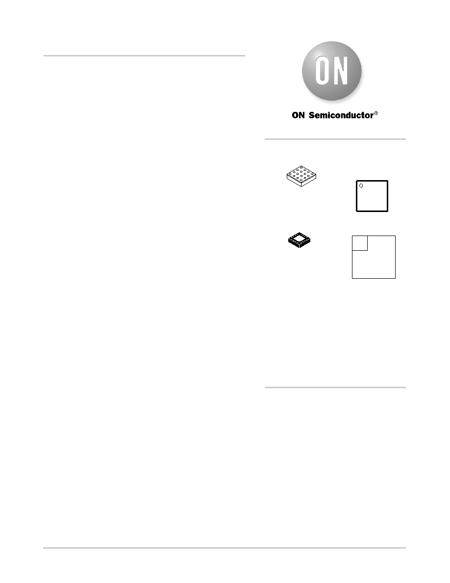
QFN16
MN SUFFIX
CASE 485G
16
SG
53A
ALYWG
G
1
1
(Note: Microdot may be in either location)
FCBGA16
BA SUFFIX
CASE 489
SG
53A
ALYWG
G
相关PDF资料 |
PDF描述 |
|---|---|
| NC7SP74L8X | IC FLIP FLOP ULP D 8-MICROPAK |
| NC7SZ175P6X_F40 | IC FLIP FLOP SGL UHS D SC70-6 |
| NC7SZ373P6 | IC LATCH UHS D 3-STATE SC70-6 |
| NC7SZ374L6X_F113 | IC FLIP FLOP UHS D 3ST 6MICROPAK |
| NC7SZ74L8X | IC FLIP FLOP UHS D 8-MICROPAK |
相关代理商/技术参数 |
参数描述 |
|---|---|
| NBSG53ABAR2 | 功能描述:触发器 2.5V/3.3V SiGe Diff RoHS:否 制造商:Texas Instruments 电路数量:2 逻辑系列:SN74 逻辑类型:D-Type Flip-Flop 极性:Inverting, Non-Inverting 输入类型:CMOS 输出类型: 传播延迟时间:4.4 ns 高电平输出电流:- 16 mA 低电平输出电流:16 mA 电源电压-最大:5.5 V 最大工作温度:+ 85 C 安装风格:SMD/SMT 封装 / 箱体:X2SON-8 封装:Reel |
| NBSG53AMA1TBG | 制造商:ON Semiconductor 功能描述:SIGE DIF CLK DATA D F-F - Tape and Reel |
| NBSG53AMAG | 功能描述:IC FLIP FLOP/CLK DIVIDER 16FCLGA RoHS:是 类别:集成电路 (IC) >> 逻辑 - 触发器 系列:- 产品变化通告:Product Discontinuation 27/Jan/2012 标准包装:2,000 系列:74LCX 功能:标准 类型:D 型总线 输出类型:三态非反相 元件数:1 每个元件的位元数:8 频率 - 时钟:150MHz 延迟时间 - 传输:1.5ns 触发器类型:正边沿 输出电流高,低:24mA,24mA 电源电压:2 V ~ 3.6 V 工作温度:-40°C ~ 85°C 安装类型:表面贴装 封装/外壳:20-SOIC(0.209",5.30mm 宽) 包装:带卷 (TR) 其它名称:MC74LCX574MELG-NDMC74LCX574MELGOSTR |
| NBSG53AMN | 功能描述:触发器 2.5V/3.3V SiGe Diff RoHS:否 制造商:Texas Instruments 电路数量:2 逻辑系列:SN74 逻辑类型:D-Type Flip-Flop 极性:Inverting, Non-Inverting 输入类型:CMOS 输出类型: 传播延迟时间:4.4 ns 高电平输出电流:- 16 mA 低电平输出电流:16 mA 电源电压-最大:5.5 V 最大工作温度:+ 85 C 安装风格:SMD/SMT 封装 / 箱体:X2SON-8 封装:Reel |
| NBSG53AMNG | 功能描述:触发器 2.5V/3.3V SiGe Diff Clock/Divider RoHS:否 制造商:Texas Instruments 电路数量:2 逻辑系列:SN74 逻辑类型:D-Type Flip-Flop 极性:Inverting, Non-Inverting 输入类型:CMOS 输出类型: 传播延迟时间:4.4 ns 高电平输出电流:- 16 mA 低电平输出电流:16 mA 电源电压-最大:5.5 V 最大工作温度:+ 85 C 安装风格:SMD/SMT 封装 / 箱体:X2SON-8 封装:Reel |
发布紧急采购,3分钟左右您将得到回复。