参数资料
| 型号: | NBSG53ABAHTBG |
| 厂商: | ON Semiconductor |
| 文件页数: | 17/18页 |
| 文件大小: | 0K |
| 描述: | IC CLOCK/DATA DIFF DIV/2 16FCBGA |
| 产品变化通告: | Product Obsolescence 05/Oct/2010 |
| 标准包装: | 100 |
| 功能: | 复位 |
| 类型: | D 型总线 |
| 输出类型: | 差分 |
| 元件数: | 1 |
| 每个元件的位元数: | 2 |
| 频率 - 时钟: | 8GHz |
| 触发器类型: | 正,负 |
| 电源电压: | 2.375 V ~ 3.465 V |
| 工作温度: | -40°C ~ 70°C |
| 安装类型: | 表面贴装 |
| 封装/外壳: | 16-LBGA,FCBGA |
| 包装: | 带卷 (TR) |
NBSG53A
http://onsemi.com
8
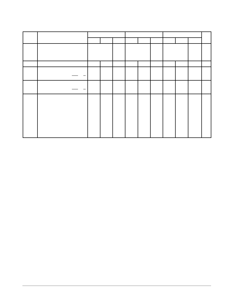
Table 9. DC CHARACTERISTICS, NECL INPUT WITH NECL OUTPUT
Symbol
Unit
70°C(BGA)/85°C(QFN)***
25°C
40°C
Characteristic
Symbol
Unit
Max
Typ
Min
Max
Typ
Min
Max
Typ
Min
Characteristic
VIHCMR
Input HIGH Voltage Common
Mode Range
(Differential Configuration)
(Note 22)
VEE + 1.2
0.0
VEE + 1.2
0.0
VEE + 1.2
0.0
V
RTIN
Internal Input Termination Resistor
45
50
55
45
50
55
45
50
55
W
IIH
Input HIGH Current (@VIH)
R, SEL
CLK, CLK, D, D
35
5
100
50
35
5
100
50
35
5
100
50
mA
IIL
Input LOW Current (@VIL)
R, SEL
CLK, CLK, D, D
20
5
100
50
20
5
100
50
20
5
100
50
mA
IOLS
OLS Input Current
(See Figure 12)
(OLS = VCC)
(OLS = VCC 0.4 V)
(OLS = VCC 0.8 V,
OLS = FLOAT)
(OLS = VCC 1.2 V)
3.465 V v VEE v 3.0 V
*(OLS = VEE)
3.0 V < VEE v 2.375 V
(OLS = VEE)
300
1500
1000
300
100
5
100
600
400
900
300
100
300
1500
1000
300
100
5
100
600
400
900
300
100
300
1500
1000
300
100
5
100
600
400
900
300
100
mA
NOTE: Device will meet the specifications after thermal equilibrium has been established when mounted in a test socket or printed circuit
board with maintained transverse airflow greater than 500 lfpm. Electrical parameters are guaranteed only over the declared
operating temperature range. Functional operation of the device exceeding these conditions is not implied. Device specification
limit values are applied individually under normal operating conditions and not valid simultaneously.
20.Input and output parameters vary 1:1 with VCC.
21.All outputs loaded with 50 W to VCC 2.0 V.
22.VIHCMR min varies 1:1 with VEE, VIHCMR max varies 1:1 with VCC. The VIHCMR range is referenced to the most positive side of the differential
input signal.
23.VIH cannot exceed VCC. |VIH VTHR| < 2600 mV.
24.VIL always w VEE. |VIL VTHR| < 2600 mV.
25.VTHR is the voltage applied to one input when running in singleended mode.
*Typicals used for testing purposes.
**When an output level of 400 mV is desired and VCC VEE > 3.0 V, a 2 kW resistor should be connected from OLS to VEE.
***The device packaged in FCBGA16 have maximum ambient temperature specification of 70°C and devices packaged in QFN16 have
maximum ambient temperature specification of 85°C.
相关PDF资料 |
PDF描述 |
|---|---|
| NC7SP74L8X | IC FLIP FLOP ULP D 8-MICROPAK |
| NC7SZ175P6X_F40 | IC FLIP FLOP SGL UHS D SC70-6 |
| NC7SZ373P6 | IC LATCH UHS D 3-STATE SC70-6 |
| NC7SZ374L6X_F113 | IC FLIP FLOP UHS D 3ST 6MICROPAK |
| NC7SZ74L8X | IC FLIP FLOP UHS D 8-MICROPAK |
相关代理商/技术参数 |
参数描述 |
|---|---|
| NBSG53ABAR2 | 功能描述:触发器 2.5V/3.3V SiGe Diff RoHS:否 制造商:Texas Instruments 电路数量:2 逻辑系列:SN74 逻辑类型:D-Type Flip-Flop 极性:Inverting, Non-Inverting 输入类型:CMOS 输出类型: 传播延迟时间:4.4 ns 高电平输出电流:- 16 mA 低电平输出电流:16 mA 电源电压-最大:5.5 V 最大工作温度:+ 85 C 安装风格:SMD/SMT 封装 / 箱体:X2SON-8 封装:Reel |
| NBSG53AMA1TBG | 制造商:ON Semiconductor 功能描述:SIGE DIF CLK DATA D F-F - Tape and Reel |
| NBSG53AMAG | 功能描述:IC FLIP FLOP/CLK DIVIDER 16FCLGA RoHS:是 类别:集成电路 (IC) >> 逻辑 - 触发器 系列:- 产品变化通告:Product Discontinuation 27/Jan/2012 标准包装:2,000 系列:74LCX 功能:标准 类型:D 型总线 输出类型:三态非反相 元件数:1 每个元件的位元数:8 频率 - 时钟:150MHz 延迟时间 - 传输:1.5ns 触发器类型:正边沿 输出电流高,低:24mA,24mA 电源电压:2 V ~ 3.6 V 工作温度:-40°C ~ 85°C 安装类型:表面贴装 封装/外壳:20-SOIC(0.209",5.30mm 宽) 包装:带卷 (TR) 其它名称:MC74LCX574MELG-NDMC74LCX574MELGOSTR |
| NBSG53AMN | 功能描述:触发器 2.5V/3.3V SiGe Diff RoHS:否 制造商:Texas Instruments 电路数量:2 逻辑系列:SN74 逻辑类型:D-Type Flip-Flop 极性:Inverting, Non-Inverting 输入类型:CMOS 输出类型: 传播延迟时间:4.4 ns 高电平输出电流:- 16 mA 低电平输出电流:16 mA 电源电压-最大:5.5 V 最大工作温度:+ 85 C 安装风格:SMD/SMT 封装 / 箱体:X2SON-8 封装:Reel |
| NBSG53AMNG | 功能描述:触发器 2.5V/3.3V SiGe Diff Clock/Divider RoHS:否 制造商:Texas Instruments 电路数量:2 逻辑系列:SN74 逻辑类型:D-Type Flip-Flop 极性:Inverting, Non-Inverting 输入类型:CMOS 输出类型: 传播延迟时间:4.4 ns 高电平输出电流:- 16 mA 低电平输出电流:16 mA 电源电压-最大:5.5 V 最大工作温度:+ 85 C 安装风格:SMD/SMT 封装 / 箱体:X2SON-8 封装:Reel |
发布紧急采购,3分钟左右您将得到回复。