- 您现在的位置:买卖IC网 > PDF目录8459 > NC7ST08P5X (Fairchild Semiconductor)IC GATE AND HST 2INPUT TTL SC70- PDF资料下载
参数资料
| 型号: | NC7ST08P5X |
| 厂商: | Fairchild Semiconductor |
| 文件页数: | 6/8页 |
| 文件大小: | 0K |
| 描述: | IC GATE AND HST 2INPUT TTL SC70- |
| 产品变化通告: | Mold Compound Change 12/Dec/2007 |
| 标准包装: | 1 |
| 系列: | 7ST |
| 逻辑类型: | 与门 |
| 电路数: | 1 |
| 输入数: | 2 |
| 电源电压: | 4.5 V ~ 5.5 V |
| 电流 - 静态(最大值): | 1µA |
| 输出电流高,低: | 2mA,2mA |
| 逻辑电平 - 低: | 0.8V |
| 逻辑电平 - 高: | 2V |
| 额定电压和最大 CL 时的最大传播延迟: | 26ns @ 5.5V,50pF |
| 工作温度: | -40°C ~ 85°C |
| 安装类型: | 表面贴装 |
| 供应商设备封装: | SC-70-5 |
| 封装/外壳: | 6-TSSOP(5 引线),SC-88A,SOT-353 |
| 包装: | 标准包装 |
| 产品目录页面: | 1223 (CN2011-ZH PDF) |
| 其它名称: | NC7ST08P5XDKR |
2006 Fairchild Semiconductor
www.fairchildsemi.com
FMS6346 Rev. 1.0.5
6
FMS6346
—
Six
Channel,
6th-Order
SD/HD
V
ideo
FIlter
Driver
YOUT
Driver
YIN
0.65V
800k
Ω
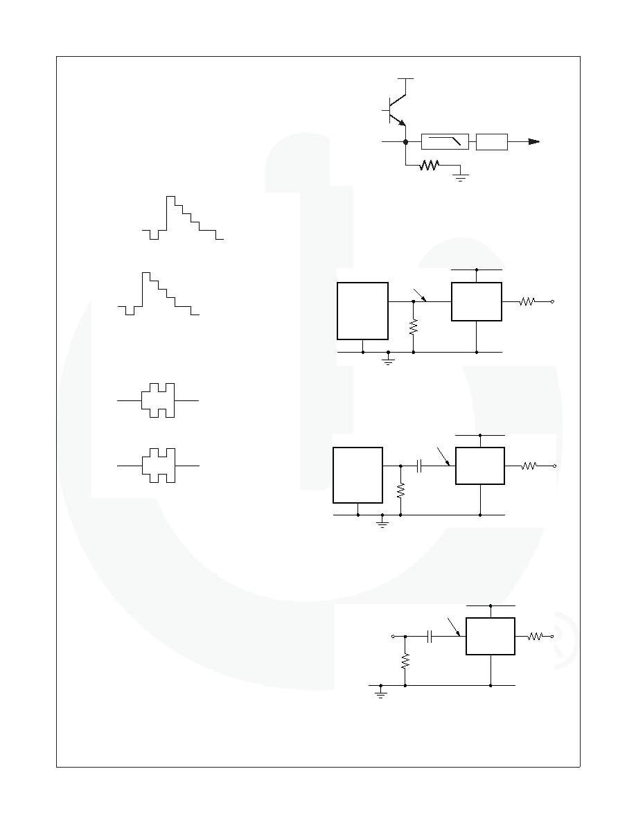
Applications Information
Functional Description
The FMS6346 Low-Cost Video Filter (LCVF) provides
6dB gain from input to output. In addition, the input is
slightly offset to optimize the output driver performance.
The offset is held to the minimum required value to de-
crease the standing DC current into the load. Typical volt-
age levels are shown in Figure 11.
Figure 11. Typical Voltage Levels
The FMS6346 provides an internal diode clamp to sup-
port AC-coupled input signals. If the input signal does not
go below ground, the input clamp does not operate. This
allows DAC outputs to directly drive the FMS6346 without
an AC coupling capacitor. The worst-case sync tip com-
pression due to the clamp does not exceed 7mV. The in-
put level set by the clamp, combined with the internal DC
offset, keeps the output within its acceptable range. When
the input is AC-coupled, the diode clamp sets the sync tip
(or lowest voltage) just below ground.
For symmetric signals like C, U, V, Cb, Cr, Pb, and Pr; the
average DC bias is fairly constant and the inputs can be
AC-coupled with the addition of a pull-up resistor to set
the DC input voltage. DAC outputs can also drive these
same signals without the AC coupling capacitor. A con-
ceptual illustration of the input clamp circuit is shown in
Figure 12.
Figure 12. Input Clamp Circuit
I/O Congurations
For DC-coupled DAC drive with DC-coupled outputs, use
the conguration shown in Figure 13.
Figure 13. DC-Coupled Inputs and Outputs
If the DAC’s average DC output level causes the signal to
exceed the range of 0V to 1.4V, it can be AC-coupled as
shown in Figure 14.
Figure 14. AC-Coupled Inputs, DC-Coupled Outputs
When the is driven by an unknown external source or a
SCART switch with its own clamping circuitry, the inputs
should be AC-coupled as shown in Figure 15.
Figure 15. SCART Conguration with DC-Coupled
Outputs
There is a 280mV offset from the DC input level to the
DC output level. VOUT = 2 * VIN + 280mV.
0.0 -> 0.02V
0.3 -> 0.32V
0.65 -> 0.67V
1.0 -> 1.02V
VIN
0.28V
0.88V
1.58V
2.28V
Driven by:
DC-Coupled DAC Outputs
AC-Coupled and Clamped
Y, CV, R, G, B
VOUT
0.15V
0.5V
0.85V
VIN
0.58V
1.28V
1.98V
Driven by:
AC-Coupled and Biased
U, V, Pb, Pr, C
VOUT
DVD or
STB
SoC
DAC
Output
75Ω
LCVF
Clamp
Inactive
0V - 1.4V
DVD or
STB
SoC
DAC
Output
75Ω
LCVF
Clamp
Inactive
0V - 1.4V
DVD or
STB
SoC
DAC
Output
LCVF
Clamp
Active
0.1μF
0V - 1.4V
75Ω
DVD or
STB
SoC
DAC
Output
LCVF
Clamp
Active
0.1μF
0V - 1.4V
75Ω
LCVF
Clamp
Active
0.1μF
External video
source must
be AC coupled
0V - 1.4V
75Ω
LCVF
Clamp
Active
0.1μF
External video
source must
be AC coupled
0V - 1.4V
75Ω
相关PDF资料 |
PDF描述 |
|---|---|
| 6257 | 7/16 DIN MALE/N FEMALE |
| 6260 | 7/16 DIN FEMALE/N FEMALE |
| VE-B43-MU-F4 | CONVERTER MOD DC/DC 24V 200W |
| SN74AHCT595NSRG4 | IC SHIFT REGISTER SGL 8B 16SOP |
| 6863 | ADAPTER XLR FEMALE/1/4" PLUG |
相关代理商/技术参数 |
参数描述 |
|---|---|
| NC7ST08P5X_NL | 功能描述:逻辑门 FINISHED GOOD RoHS:否 制造商:Texas Instruments 产品:OR 逻辑系列:LVC 栅极数量:2 线路数量(输入/输出):2 / 1 高电平输出电流:- 16 mA 低电平输出电流:16 mA 传播延迟时间:3.8 ns 电源电压-最大:5.5 V 电源电压-最小:1.65 V 最大工作温度:+ 125 C 安装风格:SMD/SMT 封装 / 箱体:DCU-8 封装:Reel |
| NC7ST08P5X_Q | 功能描述:逻辑门 2-Input AND Gate RoHS:否 制造商:Texas Instruments 产品:OR 逻辑系列:LVC 栅极数量:2 线路数量(输入/输出):2 / 1 高电平输出电流:- 16 mA 低电平输出电流:16 mA 传播延迟时间:3.8 ns 电源电压-最大:5.5 V 电源电压-最小:1.65 V 最大工作温度:+ 125 C 安装风格:SMD/SMT 封装 / 箱体:DCU-8 封装:Reel |
| NC7ST32 | 制造商:FAIRCHILD 制造商全称:Fairchild Semiconductor 功能描述:TinyLogic HST 2-Input OR Gate |
| NC7ST32_04 | 制造商:FAIRCHILD 制造商全称:Fairchild Semiconductor 功能描述:TinyLogic HST 2-Input OR Gate |
| NC7ST32L6X | 功能描述:逻辑门 2-Input OR Gate RoHS:否 制造商:Texas Instruments 产品:OR 逻辑系列:LVC 栅极数量:2 线路数量(输入/输出):2 / 1 高电平输出电流:- 16 mA 低电平输出电流:16 mA 传播延迟时间:3.8 ns 电源电压-最大:5.5 V 电源电压-最小:1.65 V 最大工作温度:+ 125 C 安装风格:SMD/SMT 封装 / 箱体:DCU-8 封装:Reel |
发布紧急采购,3分钟左右您将得到回复。