- 您现在的位置:买卖IC网 > PDF目录8459 > NC7ST08P5X (Fairchild Semiconductor)IC GATE AND HST 2INPUT TTL SC70- PDF资料下载
参数资料
| 型号: | NC7ST08P5X |
| 厂商: | Fairchild Semiconductor |
| 文件页数: | 7/8页 |
| 文件大小: | 0K |
| 描述: | IC GATE AND HST 2INPUT TTL SC70- |
| 产品变化通告: | Mold Compound Change 12/Dec/2007 |
| 标准包装: | 1 |
| 系列: | 7ST |
| 逻辑类型: | 与门 |
| 电路数: | 1 |
| 输入数: | 2 |
| 电源电压: | 4.5 V ~ 5.5 V |
| 电流 - 静态(最大值): | 1µA |
| 输出电流高,低: | 2mA,2mA |
| 逻辑电平 - 低: | 0.8V |
| 逻辑电平 - 高: | 2V |
| 额定电压和最大 CL 时的最大传播延迟: | 26ns @ 5.5V,50pF |
| 工作温度: | -40°C ~ 85°C |
| 安装类型: | 表面贴装 |
| 供应商设备封装: | SC-70-5 |
| 封装/外壳: | 6-TSSOP(5 引线),SC-88A,SOT-353 |
| 包装: | 标准包装 |
| 产品目录页面: | 1223 (CN2011-ZH PDF) |
| 其它名称: | NC7ST08P5XDKR |
2006 Fairchild Semiconductor
www.fairchildsemi.com
FMS6346 Rev. 1.0.5
7
FMS6346
—
Six
Channel,
6th-Order
SD/HD
V
ideo
FIlter
Driver
The same method can be used for biased signals with the
addition of a pull-up resistor to make sure the clamp never
operates. The internal pull-down resistance is 800k
Ω
±20%, so the external resistance should be 7.5M
Ω to set
the DC level to 500mV. If a pull-up resistance less than
7.5M
Ω is desired, an external pull-down can be added
such that the DC input level is set to 500mV.
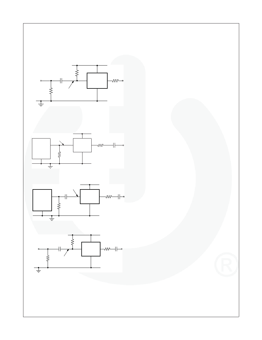
Figure 16. Biased SCART with DC-Coupled Outputs
The same circuits can be used with AC-coupled outputs if
desired, as shown in Figure 17.
Figure 17 DC-Coupled Inputs, AC-Coupled Outputs
Figure 18. AC-Coupled Inputs, AC-Coupled Outputs
Figure 19. Biased SCART with AC-Coupled Outputs
NOTE: The video tilt or line time distortion is dominated by
the AC-coupling capacitor. The value may need to be in-
creased beyond 220μF to obtain satisfactory operation in
some applications.
Power Dissipation
The FMS6346 output drive conguration must be consid-
ered when calculating overall power dissipation. Care
must be taken not to exceed the maximum die junction
temperature. The following example can be used to calcu-
late the FMS6346’s power dissipation and internal tem-
perature rise:
T
J = TA + Pd θJA
where P
d = PCH1 + PCH2 + PCHx
and P
CHx = Vs ICH - (VO
2
/R
L)
where
V
O = 2Vin + 0.280V
I
CH = (ICC / 6) +
(V
O/RL)
V
IN = RMS value of input signal
I
CC = 60mA
V
s = 5V
R
L = channel load resistance
Board layout can affect thermal characteristics. Refer to
the Layout Considerations section for more information.
Layout Considerations
General layout and supply bypassing play major roles in
high-frequency performance and thermal characteristics.
Fairchild offers a demonstration board, FMS6346DEMO,
to guide layout and aid device testing and characteriza-
tion. The FMS6346DEMO is a four-layer board with a full
power and ground plane. Following this layout congura-
tion provides the optimum performance and thermal char-
acteristics. For best results, follow the steps below as a
basis for high-frequency layout:
Include 10μF and 0.1μF ceramic bypass capacitors
Place the 10μF capacitor within 0.75 inches of the
power pin
Place the 0.1μF capacitor within 0.1 inches of the
power pin
For multi-layer boards, use a large ground plane to
help dissipate heat
For two-layer boards, use a ground plane that extends
beyond the device by at least 0.5 inches
Minimize all trace lengths to reduce series inductances
Output Considerations
The FMS6346 outputs are DC offset from the input by
150mV. Therefore, V
OUT = 2VIN DC+150mV. This offset is
required to obtain optimal performance from the output
driver and is held at the minimum value to decrease the
standing DC current into the load. Since the FMS6346
has a 2x (6dB) gain, the output is typically connected via a
75Ω-series back-matching resistor, followed by the 75Ω
video cable. Due to the inherent divide by two of this con-
guration, the blanking level at the load of the video signal
is always less than 1V. When AC-coupling the output,
ensure that the coupling capacitor of choice passes the
lowest frequency content in the video signal and that line
time distortion (video tilt) is kept as low as possible.
LCVF
Bias
Input
0.1μF
External video
source must
be AC coupled
500mV +/-350mV
75Ω
7.5MΩ
75Ω
DVD or
STB
SoC
DAC
Output
LCVF
Clamp
Inactive
0V - 1.4V
220F
75Ω
DVD or
STB
SoC
DAC
Output
LCVF
Clamp
Active
0.1μF
0V - 1.4V
75Ω
220μF
LCVF
Clamp
Active
0.1
μF
External video
source must
be AC coupled.
500mV +/-350mV
220
μF
75Ω
7.5MΩ
75Ω
相关PDF资料 |
PDF描述 |
|---|---|
| 6257 | 7/16 DIN MALE/N FEMALE |
| 6260 | 7/16 DIN FEMALE/N FEMALE |
| VE-B43-MU-F4 | CONVERTER MOD DC/DC 24V 200W |
| SN74AHCT595NSRG4 | IC SHIFT REGISTER SGL 8B 16SOP |
| 6863 | ADAPTER XLR FEMALE/1/4" PLUG |
相关代理商/技术参数 |
参数描述 |
|---|---|
| NC7ST08P5X_NL | 功能描述:逻辑门 FINISHED GOOD RoHS:否 制造商:Texas Instruments 产品:OR 逻辑系列:LVC 栅极数量:2 线路数量(输入/输出):2 / 1 高电平输出电流:- 16 mA 低电平输出电流:16 mA 传播延迟时间:3.8 ns 电源电压-最大:5.5 V 电源电压-最小:1.65 V 最大工作温度:+ 125 C 安装风格:SMD/SMT 封装 / 箱体:DCU-8 封装:Reel |
| NC7ST08P5X_Q | 功能描述:逻辑门 2-Input AND Gate RoHS:否 制造商:Texas Instruments 产品:OR 逻辑系列:LVC 栅极数量:2 线路数量(输入/输出):2 / 1 高电平输出电流:- 16 mA 低电平输出电流:16 mA 传播延迟时间:3.8 ns 电源电压-最大:5.5 V 电源电压-最小:1.65 V 最大工作温度:+ 125 C 安装风格:SMD/SMT 封装 / 箱体:DCU-8 封装:Reel |
| NC7ST32 | 制造商:FAIRCHILD 制造商全称:Fairchild Semiconductor 功能描述:TinyLogic HST 2-Input OR Gate |
| NC7ST32_04 | 制造商:FAIRCHILD 制造商全称:Fairchild Semiconductor 功能描述:TinyLogic HST 2-Input OR Gate |
| NC7ST32L6X | 功能描述:逻辑门 2-Input OR Gate RoHS:否 制造商:Texas Instruments 产品:OR 逻辑系列:LVC 栅极数量:2 线路数量(输入/输出):2 / 1 高电平输出电流:- 16 mA 低电平输出电流:16 mA 传播延迟时间:3.8 ns 电源电压-最大:5.5 V 电源电压-最小:1.65 V 最大工作温度:+ 125 C 安装风格:SMD/SMT 封装 / 箱体:DCU-8 封装:Reel |
发布紧急采购,3分钟左右您将得到回复。