- 您现在的位置:买卖IC网 > Datasheet目录996 > NCP1028LEDGEVB (ON Semiconductor)EVAL BOARD FOR NCP1028LEDG Datasheet资料下载
参数资料
| 型号: | NCP1028LEDGEVB |
| 厂商: | ON Semiconductor |
| 文件页数: | 25/29页 |
| 文件大小: | 0K |
| 描述: | EVAL BOARD FOR NCP1028LEDG |
| 设计资源: | NCP1028LEDGEVB BOM CP1028LEDGEVB Gerber Files NCP1028LED EVB Schematic |
| 标准包装: | 1 |
| 电流 - 输出 / 通道: | 720mA |
| 输出及类型: | 1,隔离 |
| 输出电压: | 18V |
| 输入电压: | 90 ~ 265VAC |
| 已供物品: | 板 |
| 已用 IC / 零件: | NCP1028 |
| 其它名称: | NCP1028LEDGEVBOS |
第1页第2页第3页第4页第5页第6页第7页第8页第9页第10页第11页第12页第13页第14页第15页第16页第17页第18页第19页第20页第21页第22页第23页第24页当前第25页第26页第27页第28页第29页
�� �
�
�NCP1028�
�L� +�
�+� 3.8� mH�
�+� 120�
�0.49� +� 258� mA� peak� *� to� *� peak�
�D� IL� +�
�+� 0.447�
�40n� +� 130� mW�
�Poff� +�
�+� Ipeak� +� 156m� )�
�Ipeak� +�
�Iavg� D� IL� D� IL�
�)� +� 447� mA�
�I1� +� Ipeak-�
�D� IL�
�+� 0.447-0.129� +� 318� mA�
�Pon� +�
�+� 0.447�
�40n� +� 22� mW�
�?� Large� K:� approaching� BCM� where� the� rms� losses� are�
�the� worse,� but� smaller� inductance,� leading� to� a� better�
�leakage� inductance.�
�From� Equation� 16,� a� K� factor� of� 0.8� (40%� ripple),� gives�
�an� inductance� of:�
�(120� 0.49)2�
�60k� 0.8� 18.75�
�Vind�
�LFSW� 3.8m� 60k�
�The� peak� current� can� be� evaluated� to� be:�
�d� 2� 0.49� 2�
�In� Figure� 43,� I� 1� can� also� be� calculated:�
�2�
�5.� Based� on� the� above� numbers,� we� can� now�
�evaluate� the� conduction� losses:�
�If� we� take� the� maximum� R� DS(on)� for� a� 120� °� C� junction�
�temperature,� i.e.� 11� W� ,� then� conduction� losses� worse� case�
�are:�
�Pcond� +� I2d,� rms� Rds(on)� +� 571� mW�
�6.� Off-time� and� on-time� switching� losses� can� be�
�estimated� based� on� the� following� calculations:�
�IpeakVdstoff� 650�
�6TSW� 6� 15u�
�(eq.� 18)�
�IpeakN(Vout� )� Vf)ton�
�6TSW� (eq.� 19)�
�114�
�6� 15u�
�The� theoretical� total� power� is� then� 0.571� +� 0.13� +� 0.022�
�=� 723� mW.�
�7.� The� ramp� compensation� will� be� calculated� as�
�suggested� by� Equation� 13� giving� a� resistor� of�
�78� k� W� or� 82� k� W� for� the� normalized� value.�
�1� )� 1�
�2� +� 228� mA� rms�
�HV�
�3� 2� 0.318�
�0.258�
�Id,� rms� +� I1� d� 1� )� 1� D� IL� 2� +� 0.318�
�3� 2I1�
�0.7�
�HV�
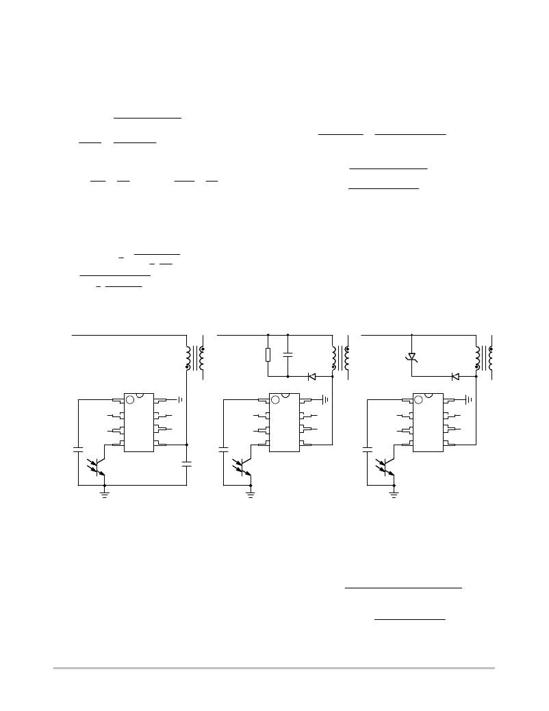
�Power� Switch� Circuit� Protection�
�As� in� any� Flyback� design,� it� is� important� to� limit� the� drain�
�excursion� to� a� safe� value,� e.g.� below� the� power� switch�
�circuit� BVdss� which� is� 700� V.� Figures� 44a,� b,� c� present�
�possible� implementations:�
�HV�
�R� clamp�
�C� clamp�
�D�
�Dz�
�D�
�1�
�2�
�3�
�8�
�7�
�6�
�1�
�2�
�3�
�8�
�7�
�6�
�1�
�2�
�3�
�8�
�7�
�6�
�CV� CC� +�
�4�
�5�
�CV� CC� +�
�4�
�5�
�CV� CC� +�
�4�
�5�
�C�
�a.�
�b.�
�Figure� 44.� Different� Options� to� Clamp� the� Leakage� Spike�
�c.�
�Figure� 44a:� The� simple� capacitor� limits� the� voltage�
�according� to� Equation� 14.� This� option� is� only� valid� for� low�
�power� applications,� e.g.� below� 5.0� W,� otherwise� chances�
�Figure� 44b:� The� most� standard� circuitry� called� the� RCD�
�network.� You� calculate� R� clamp� and� C� clamp� using� the�
�following� formulae:�
�exist� to� destroy� the� MOSFET.� After� evaluating� the� leakage�
�inductance,� you� can� compute� C� with� Equation� 15.� Typical�
�values� are� between� 100� pF� and� up� to� 470� pF.� Large�
�Rclamp� +�
�2Vclamp(Vclamp-(Vout� )� Vf)� N)�
�LpeakI2peak� FSW�
�(eq.� 20)�
�capacitors� increase� capacitive� losses� …�
�Cclamp� +�
�Vclamp�
�VrippleFSWRclamp�
�(eq.� 21)�
�http://onsemi.com�
�25�
�相关PDF资料 |
PDF描述 |
|---|---|
| NCP1216AFORWGEVB | BOARD EVAL NCP1216A 35W |
| NCP1351LEDGEVB | EVAL BOARD FOR NCP1351LEDG |
| NCP3065BBGEVB | BOARD EVAL NCP3065 MR16 BOOST |
| NCP3066SCBCKGEVB | EVAL BOARD FOR NCP3066SCBCKG |
| NCP5005GEVB | EVAL BOARD FOR NCP5005G |
相关代理商/技术参数 |
参数描述 |
|---|---|
| NCP1028P065G | 功能描述:电流型 PWM 控制器 NCP1028 65 KHZ RoHS:否 制造商:Texas Instruments 开关频率:27 KHz 上升时间: 下降时间: 工作电源电压:6 V to 15 V 工作电源电流:1.5 mA 输出端数量:1 最大工作温度:+ 105 C 安装风格:SMD/SMT 封装 / 箱体:TSSOP-14 |
| NCP1028P100G | 功能描述:电流型 PWM 控制器 NCP1028 100 KHZ RoHS:否 制造商:Texas Instruments 开关频率:27 KHz 上升时间: 下降时间: 工作电源电压:6 V to 15 V 工作电源电流:1.5 mA 输出端数量:1 最大工作温度:+ 105 C 安装风格:SMD/SMT 封装 / 箱体:TSSOP-14 |
| NCP1028PL065R2G | 功能描述:交流/直流开关转换器 ANA 1 FREQ GULLWING RoHS:否 制造商:STMicroelectronics 输出电压:800 V 输入/电源电压(最大值):23.5 V 输入/电源电压(最小值):11.5 V 开关频率:115 kHz 电源电流:1.6 mA 工作温度范围:- 40 C to + 150 C 安装风格:SMD/SMT 封装 / 箱体:SSO-10 封装:Reel |
| NCP102MBGEVB | 功能描述:电源管理IC开发工具 NCP102 4W MOTHERBRD EVB RoHS:否 制造商:Maxim Integrated 产品:Evaluation Kits 类型:Battery Management 工具用于评估:MAX17710GB 输入电压: 输出电压:1.8 V |
| NCP102SNT1G | 功能描述:低压差稳压器 - LDO LDO LINR REG CONTRL RoHS:否 制造商:Texas Instruments 最大输入电压:36 V 输出电压:1.4 V to 20.5 V 回动电压(最大值):307 mV 输出电流:1 A 负载调节:0.3 % 输出端数量: 输出类型:Fixed 最大工作温度:+ 125 C 安装风格:SMD/SMT 封装 / 箱体:VQFN-20 |
发布紧急采购,3分钟左右您将得到回复。