- 您现在的位置:买卖IC网 > PDF目录19623 > NCP1230P65G (ON Semiconductor)IC CTRLR PWM SMPS OVP OCP 7DIP PDF资料下载
参数资料
| 型号: | NCP1230P65G |
| 厂商: | ON Semiconductor |
| 文件页数: | 12/21页 |
| 文件大小: | 0K |
| 描述: | IC CTRLR PWM SMPS OVP OCP 7DIP |
| 标准包装: | 50 |
| 输出隔离: | 隔离 |
| 频率范围: | 65kHz |
| 输入电压: | 8.4 V ~ 18 V |
| 工作温度: | -40°C ~ 125°C |
| 封装/外壳: | 8-DIP(0.300",7.62mm),7 引线 |
| 供应商设备封装: | 7-PDIP |
| 包装: | 管件 |
�� �
�
�NCP1230�
�Ipk� +� 0.75�
�Feedback�
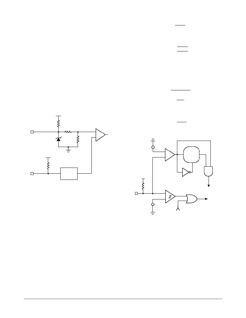
�The� feedback� pin� has� been� designed� to� be� connected�
�directly� to� the� open� ?� collector� output� of� an� optocoupler.� The�
�pin� is� pulled� ?� up� through� a� 20� k� W� resistor� to� the� internal�
�Vdd_fb� supply� (5� volts� nominal).� The� feedback� input� signal�
�where:�
�Rs� @� 3�
�Ipk� @� Rs� +� 1V�
�2� @� Pin�
�Lp� @� f�
�is� divided� down,� by� a� factor� of� three,� and� connected� to� the�
�negative� (� ?� )� input� of� the� PWM� comparator.� The� positive� (+)�
�input� to� the� PWM� comparator� is� the� current� sense� signal�
�(Figure� 30).�
�The� NCP1230� is� a� peak� current� mode� controller,� where�
�the� feedback� signal� is� proportional� to� the� output� power.� At�
�the� beginning� of� the� cycle,� the� power� switch� is� turns� ?� on� and�
�the� current� begins� to� increase� in� the� primary� of� the�
�Ipk� +�
�where:�
�P� in� =� is� the� power� level� where� the� NCP1230� will� go� into�
�the� skip� mode�
�L� p� =� Primary� inductance�
�f� =� NCP1230� controller� frequency�
�Pin� +� p�
�Pin� +� Pout�
�transformer,� when� the� peak� current� crosses� the� feedback�
�voltage� level,� the� PWM� comparators� switches� from� a� logic�
�level� low,� to� a� logic� level� high,� resetting� the� PWM� latching�
�Flip� ?� Flop,� turning� off� the� power� switch� until� the� next�
�oscillator� clock� cycle� begins.�
�where:�
�L� @� f� @� Ipk2�
�2�
�Eff�
�Vdd_fb�
�Eff� =� the� power� supply� efficiency�
�Rout� +� Eout�
�2�
�FB�
�20k�
�55k�
�10� V�
�25k�
�?�
�+�
�PWM�
�Vskip�
�2�
�Pout�
�S� is� rising� edge� triggered�
�R� is� falling� edge� triggered�
�/� Vstby� ?� out�
�2.3� Vpp�
�Ramp�
�+�
�1.25� V�
�+�
�?�
�125� ms�
�S�
�R�
�18k�
�3�
�LEB�
�Vdd_fb�
�Figure� 30.�
�The� feedback� pin� input� is� clamped� to� a� nominal� 10� volt� for�
�ESD� protection.�
�Skip� Mode�
�FB�
�Vskip�
�+�
�0.75� V�
�?�
�+�
�PFC_V� CC�
�Latch�
�Reset�
�The� feedback� input� is� connected� in� parallel� with� the� skip�
�cycle� logic� (Figure� 31).� When� the� feedback� voltage� drops�
�below� 25%� of� the� maximum� peak� current� (1.0� V/Rsense)� the�
�IC� prevents� the� current� from� decreasing� any� further� and�
�starts� to� blank� the� output� pulses.� This� is� called� the� skip� cycle�
�mode.� While� the� controller� is� in� the� burst� mode� the� power�
�transfer� now� depends� upon� the� duty� cycle� of� the� pulse� burst�
�width� which� reduces� the� average� input� power� demand.�
�Vc� +� Ipk� @� Rs� @� 3�
�where:�
�V� c� =� control� voltage� (Feedback� pin� input),�
�I� pk� =� Peak� primary� current,�
�R� s� =� Current� sense� resistor,�
�3� =� Feedback� divider� ratio.�
�SkipLevel� +� 3V� @� 25%� +� 0.75V�
�CS� Cmp�
�Figure� 31.�
�During� the� skip� mode� the� PFC_Vcc� signal� (pin� 1)� is�
�asserted� into� a� high� impedance� state� when� a� light� load�
�condition� is� detected� and� confirmed,� Figure� 32� shows�
�typical� waveforms.� The� first� section� of� the� waveform� shows�
�a� normal� startup� condition,� where� the� output� voltage� is� low,�
�as� a� result� the� feedback� signal� will� be� high� asking� the�
�controller� to� provide� the� maximum� power� to� the� output.� The�
�second� phase� is� under� normal� loading,� and� the� output� is� in�
�regulation.� The� third� phase� is� when� the� output� power� drops�
�below� the� 25%� threshold� (the� feedback� voltage� drops� to� 0.75�
�volts).� When� this� occurs,� the� 125� msec� timer� starts,� and� if� the�
�conditions� is� still� present� after� the� time� output� period,� the�
�http://onsemi.com�
�12�
�相关PDF资料 |
PDF描述 |
|---|---|
| RCM08DTBS | CONN EDGECARD 16POS R/A .156 SLD |
| GSC40DRAS-S734 | CONN EDGECARD 80POS .100 R/A SLD |
| DEBE33A472ZA2B | CAP CER 4700PF 1KV RADIAL |
| EBM06DTAT-S189 | CONN EDGECARD 12POS R/A .156 SLD |
| EMM40DTMD | CONN EDGECARD 80POS R/A .156 SLD |
相关代理商/技术参数 |
参数描述 |
|---|---|
| NCP1231 | 制造商:ONSEMI 制造商全称:ON Semiconductor 功能描述:Low−Standby Power High Performance PWM Controller |
| NCP1231D100R2 | 制造商:ONSEMI 制造商全称:ON Semiconductor 功能描述:Low−Standby Power High Performance PWM Controller |
| NCP1231D100R2G | 制造商:ONSEMI 制造商全称:ON Semiconductor 功能描述:Low−Standby Power High Performance PWM Controller |
| NCP1231D133R2 | 制造商:ONSEMI 制造商全称:ON Semiconductor 功能描述:Low−Standby Power High Performance PWM Controller |
| NCP1231D133R2G | 制造商:ONSEMI 制造商全称:ON Semiconductor 功能描述:Low−Standby Power High Performance PWM Controller |
发布紧急采购,3分钟左右您将得到回复。