- 您现在的位置:买卖IC网 > PDF目录19586 > NCP1294EDBR2G (ON Semiconductor)IC PWM CTLR FLYBACK 16TSSOP PDF资料下载
参数资料
| 型号: | NCP1294EDBR2G |
| 厂商: | ON Semiconductor |
| 文件页数: | 11/13页 |
| 文件大小: | 0K |
| 描述: | IC PWM CTLR FLYBACK 16TSSOP |
| 标准包装: | 2,500 |
| 输出隔离: | 隔离 |
| 频率范围: | 260kHz ~ 320kHz |
| 输入电压: | 4.7 V ~ 15 V |
| 工作温度: | -40°C ~ 125°C |
| 封装/外壳: | 16-TSSOP(0.173",4.40mm 宽) |
| 供应商设备封装: | 16-TSSOP |
| 包装: | 带卷 (TR) |
�� �
�
�NCP1294�
�800�
�700�
�1.00�
�0.95�
�600�
�500�
�400�
�300�
�200�
�R� T� = 10 K�
�R� T� =� 5.0� K�
�0.90�
�0.85�
�0.80�
�0.75�
�0.70�
�0.65�
�0.60�
�100�
�0�
�0.0001�
�R� T� = 50 K�
�0.001�
�0.01�
�0.55�
�0.50�
�1000�
�10000�
�100000�
�1000000�
�C� T� (� m� F)�
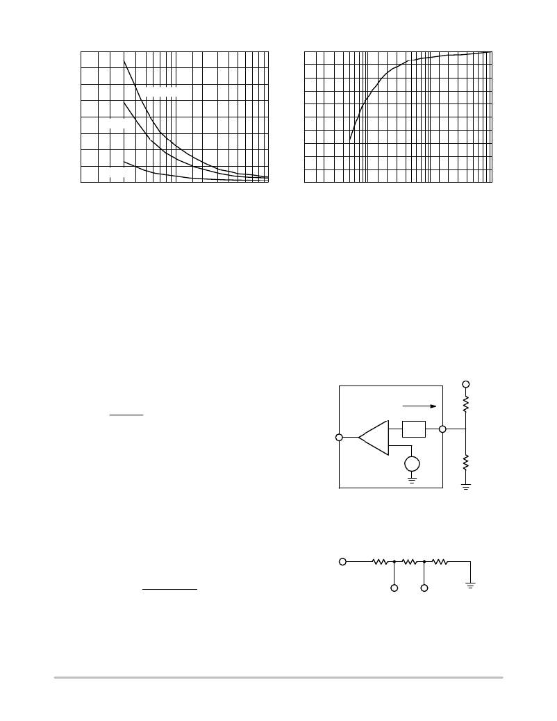
�Figure� 10.� Typical� Performance� Characteristics,�
�Oscillator� Frequency� vs.� C� T�
�that� during� steady� state,� V� COMP� doesn’t� change� for� input�
�voltage� variations.� This� intuitively� explains� why� FF� voltage�
�mode� control� has� superior� line� regulation� and� line� transient�
�response.� Knowing� the� nominal� value� of� V� IN� and� T� ON� ,� one�
�can� also� select� the� value� of� RC� to� place� V� COMP� at� the� center�
�of� its� dynamic� range.�
�Select� Feedback� Voltage� Divider�
�As� shown� in� Figure� 12,� the� voltage� divider� output� feeds� to�
�the� FB� pin,� which� connects� to� the� inverting� input� of� the� error�
�amplifier.� The� non� ?� inverting� input� of� the� error� amplifier� is�
�connected� to� a� 1.27� V� (typ)� reference� voltage.� The� FB� pin�
�has� an� input� current� which� has� to� be� considered� for� accurate�
�DC� outputs.� The� following� equation� can� be� used� to� calculate�
�R� T� (� W� )�
�Figure� 11.� Typical� Performance� Characteristics,�
�Oscillator� Duty� Cycle� vs.� R� T�
�12.5� m� A� (R1� )� R2)� +� VHYST� (C)�
�where:�
�V� IN(LOW)� ,� V� IN(HIGH)� =� input� voltage� OV� and� UV�
�threshold;�
�V� HYST� =� OV� hysteresis� seen� at� V� IN�
�It� is� self� ?� evident� from� equation� A� and� B� that� to� use� this�
�design,� V� IN(HIGH)� has� to� be� two� times� greater� than�
�V� IN(LOW)� .� Otherwise,� two� voltage� dividers� have� to� be� used�
�to� program� OV� and� UV� separately.�
�V� OUT�
�VOUT� +� 1.27� *�
�the� R1� and� R2� value�
�R2�
�R1� )� R2�
�where� ?� is� the� correction� factor� due� to� the� existence� of� the�
�FB� pin� input� current� Ier.�
�+� (Ri� )� R1� R2)Ier�
�Ri� =� DC� resistance� between� the� FB� pin� and� the� voltage�
�COMP�
�?�
�+�
�Ier�
�Ri�
�+�
�?�
�1.27�
�R1�
�FB�
�R2�
�divider� output.�
�Ier� =� V� FB� input� current,� 1.3� m� A� typical.�
�Design� Voltage� Dividers� for� OV� and� UV� Detection�
�In� Figure� 13,� the� voltage� divider� uses� three� resistors� in�
�series� to� set� OV� and� UV� threshold� seen� from� the� input�
�Figure� 12.� The� Design� of� Feedback� Voltage� Divider�
�Has� to� Consider� the� Error� Amplifier� Input� Current�
�voltage.� The� values� of� the� resistors� can� be� calculated� from�
�the� following� three� equations,� where� the� third� equation� is�
�derived� from� OV� hysteresis� requirement.�
�V� IN�
�R1�
�R2�
�R3�
�VIN(LOW)�
�R2� )� R3�
�R2� )� R3� )� R1�
�+� 1.0� V�
�(A)�
�V� UV�
�V� OV�
�VIN(HIGH)�
�R3�
�R2� )� R3� )� R1�
�+� 2.0� V�
�(B)�
�Figure� 13.� OV/UV� Monitor� Divider�
�http://onsemi.com�
�11�
�相关PDF资料 |
PDF描述 |
|---|---|
| EBM15DTMN-S189 | CONN EDGECARD 30POS R/A .156 SLD |
| PQ1U231M2ZPH | IC REG LDO 2.3V .15A SOT-23-5 |
| MIC5255-3.2BM5 TR | IC REG LDO 3.2V .15A SOT23-5 |
| VE-BTH-CX-B1 | CONVERTER MOD DC/DC 52V 75W |
| TAP226M010SRS | CAP TANT 22UF 10V 20% RADIAL |
相关代理商/技术参数 |
参数描述 |
|---|---|
| NCP1294EDR16 | 制造商:ONSEMI 制造商全称:ON Semiconductor 功能描述:Enhanced Voltage Mode PWM Controller |
| NCP1294EDR16G | 制造商:ONSEMI 制造商全称:ON Semiconductor 功能描述:Enhanced Voltage Mode PWM Controller |
| NCP1294EDR2G | 功能描述:电流型 PWM 控制器 ANA PWM VOLT MODE CNTR RoHS:否 制造商:Texas Instruments 开关频率:27 KHz 上升时间: 下降时间: 工作电源电压:6 V to 15 V 工作电源电流:1.5 mA 输出端数量:1 最大工作温度:+ 105 C 安装风格:SMD/SMT 封装 / 箱体:TSSOP-14 |
| NCP1294EDTB16G | 制造商:ONSEMI 制造商全称:ON Semiconductor 功能描述:Enhanced Voltage Mode PWM Controller |
| NCP1294EDTB16R2G | 制造商:ONSEMI 制造商全称:ON Semiconductor 功能描述:Enhanced Voltage Mode PWM Controller |
发布紧急采购,3分钟左右您将得到回复。