参数资料
| 型号: | NCP1397ADR2G |
| 厂商: | ON Semiconductor |
| 文件页数: | 6/27页 |
| 文件大小: | 0K |
| 描述: | IC REG CTRLR ISO PWM 16-SOIC |
| 标准包装: | 2,500 |
| PWM 型: | 控制器 |
| 输出数: | 1 |
| 频率 - 最大: | 560kHz |
| 占空比: | 52% |
| 电源电压: | 10.3 V ~ 20 V |
| 降压: | 无 |
| 升压: | 无 |
| 回扫: | 无 |
| 反相: | 无 |
| 倍增器: | 无 |
| 除法器: | 无 |
| Cuk: | 无 |
| 隔离: | 是 |
| 工作温度: | -40°C ~ 125°C |
| 封装/外壳: | 16-SOIC(0.154",3.90mm 宽)15 引线 |
| 包装: | 带卷 (TR) |
第1页第2页第3页第4页第5页当前第6页第7页第8页第9页第10页第11页第12页第13页第14页第15页第16页第17页第18页第19页第20页第21页第22页第23页第24页第25页第26页第27页
�� �
�
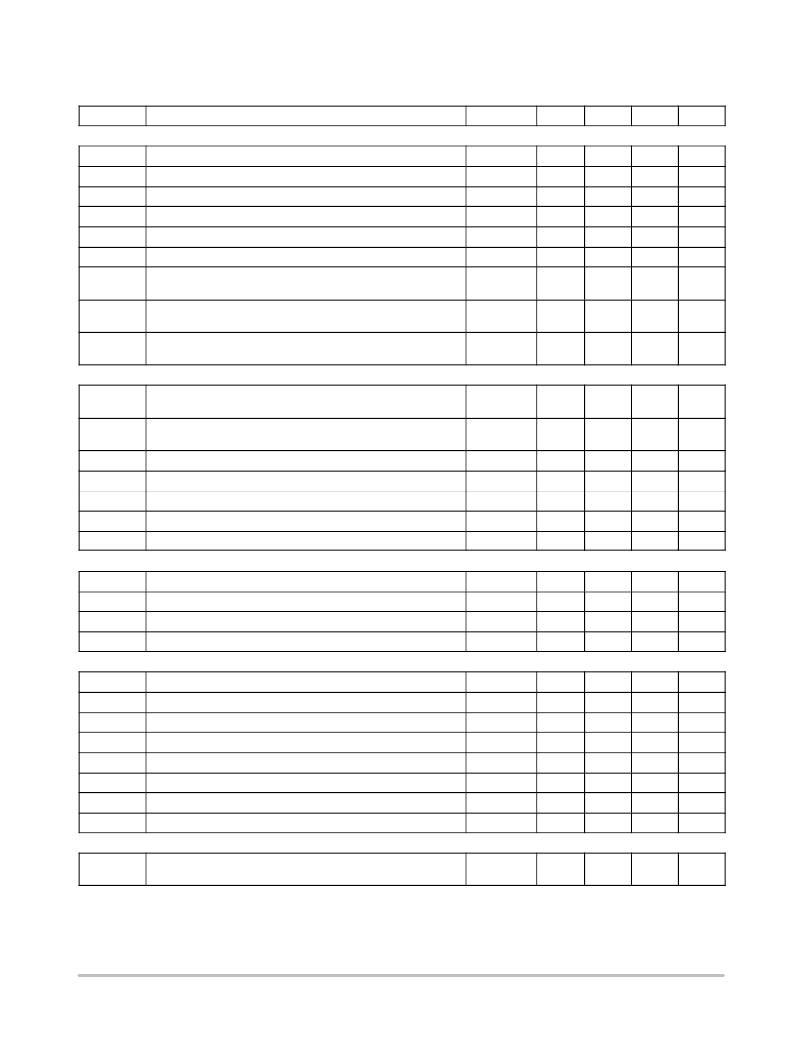
�NCP1397A,� NCP1397B�
�ELECTRICAL� CHARACTERISTICS� (For� typical� values� T� J� =� 25� °� C,� for� min/max� values� T� J� =� ?� 40� °� C� to� +125� °� C,� Max� T� J� =� 150� °� C,�
�V� CC� =� 12� V� unless� otherwise� noted)�
�Symbol�
�Rating�
�Pin�
�Min�
�Typ�
�Max�
�Unit�
�SUPPLY� SECTION�
�V� CC(on)�
�V� CC(min)�
�V� boot(on)�
�V� boot(min)�
�I� startup�
�V� CC(reset)�
�I� CC1�
�I� CC2�
�I� CC3�
�Turn� ?� on� threshold� level,� V� CC� going� up�
�Minimum� operating� voltage� after� turn� ?� on�
�Startup� voltage� on� the� floating� section�
�Cutoff� voltage� on� the� floating� section�
�Startup� current,� V� CC� <� V� CC(on)�
�V� CC� level� at� which� the� internal� logic� gets� reset�
�Internal� IC� consumption,� no� output� load� on� pin� 15/14� –� 11/10,�
�F� SW� =� 300� kHz�
�Internal� IC� consumption,� 1� nF� output� load� on� pin� 15/14� –� 11/10,�
�F� SW� =� 300� kHz�
�Consumption� in� fault� or� disable� mode� (All� drivers� disabled,�
�Rt� =� 34� k� W� ,� R� DT� =� 10� k� W� )�
�12�
�12�
�16� ?� 14�
�16� ?� 14�
�12�
�12�
�12�
�12�
�12�
�9.7�
�8.7�
�8�
�7.4�
�?�
�?�
�?�
�?�
�?�
�10.5�
�9.5�
�9�
�8.4�
�?�
�6.6�
�4�
�11�
�1.5�
�11.3�
�10.3�
�10�
�9.4�
�300�
�?�
�?�
�?�
�?�
�V�
�V�
�V�
�V�
�m� A�
�V�
�mA�
�mA�
�mA�
�VOLTAGE� CONTROL� OSCILLATOR� (VCO)�
�F� SW(min)�
�F� SW(max)�
�FB� SW�
�DC�
�T� del1�
�T� del2�
�V� ref(Rt)�
�Minimum� switching� frequency,� Rt� =� 34� k� W� on� pin� 4,� V� pin6� =� 0.8� V,�
�DT� =� 300� ns�
�Maximum� switching� frequency,� R� f(max)� =� 1.9� k� W� on� pin� 2,� V� pin6� >�
�5.3� V,� Rt� =� 34� k� W� ,� DT� =� 300� ns�
�Feedback� pin� swing� above� which� D� f� =� 0�
�Operating� duty� ?� cycle� symmetry�
�Delay� before� driver� restart� from� fault� or� disable� mode�
�Delay� before� driver� restart� after� V� CC(on)� event� (Note� 4)�
�Reference� voltage� for� Rt� pin�
�4�
�2�
�6�
�11� ?� 15�
�?�
�?�
�4�
�58.2�
�440�
�?�
�48�
�?�
�?�
�2.18�
�60�
�500�
�5.3�
�50�
�700�
�11�
�2.3�
�61.8�
�560�
�?�
�52�
�?�
�?�
�2.42�
�kHz�
�kHz�
�V�
�%�
�ns�
�m� s�
�V�
�FEEDBACK� SECTION�
�R� FB�
�V� FB(min)�
�V� FB(off)�
�V� FBoff(hyste)�
�Internal� pulldown� resistor�
�Voltage� on� pin� 6� below� which� the� FB� level� has� no� VCO� action�
�Voltage� on� pin� 6� below� which� the� controller� considers� the� FB� fault�
�Feedback� fault� comparator� hysteresis�
�6�
�6�
�6�
�6�
�?�
�?�
�240�
�?�
�20�
�1.1�
�280�
�45�
�?�
�?�
�320�
�?�
�k� W�
�V�
�mV�
�mV�
�DRIVE� OUTPUT�
�T� r�
�T� f�
�R� OH�
�R� OL�
�T� dead�
�T� dead(max)�
�T� dead(min)�
�I� HV(LEAK)�
�Output� voltage� risetime� @� C� L� =� 1� nF,� 10� ?� 90%� of� output� signal�
�Output� voltage� falltime� @� C� L� =� 1� nF,� 10� ?� 90%� of� output� signal�
�Source� resistance�
�Sink� resistance�
�Deadtime� with� R� DT� =� 10� k� W� from� pin� 7� to� GND�
�Maximum� deadtime� with� R� DT� =� 82� k� W� from� pin� 7� to� GND�
�Minimum� deadtime,� R� DT� =� 3� k� W� from� pin� 7� to� GND�
�Leakage� current� on� high� voltage� pins� to� GND�
�15� ?� 14/11� ?� 10�
�15� ?� 14/11� ?� 10�
�15� ?� 14/11� ?� 10�
�15� ?� 14/11� ?� 10�
�7�
�7�
�7�
�14,� 15,16�
�?�
�?�
�?�
�?�
�250�
�?�
�?�
�?�
�40�
�20�
�13�
�5.5�
�290�
�2�
�100�
�?�
�?�
�?�
�?�
�?�
�340�
�?�
�?�
�5�
�ns�
�ns�
�W�
�W�
�ns�
�m� s�
�ns�
�m� A�
�TIMERS�
�I� timer1�
�Timer� capacitor� charge� current� during� feedback� fault� or� when�
�V� ref(fault)� <� V� pin9� <� V� ref(OCP)�
�3�
�150�
�175�
�190�
�m� A�
�3.� The� IC� does� not� activate� soft� ?� start� (unless� the� feedback� pin� voltage� is� below� 0.3� V)� when� the� skip/disable� input� is� released,� this� is� for� skip�
�cycle� implementation.�
�4.� Guaranteed� by� design.�
�http://onsemi.com�
�6�
�相关PDF资料 |
PDF描述 |
|---|---|
| NCP1417DMR2 | IC REG BST SYNC ADJ 0.2A 8MICRO |
| NCP1421DMR2 | IC REG BST SYNC ADJ 0.6A 8MICRO |
| NCP1450ASN50T1G | IC REG CTRLR BST PWM VM 5TSOP |
| NCP1521BMUTBG | IC REG BUCK SYNC ADJ 0.6A 6UDFN |
| NCP1522ASNT1G | IC REG BUCK SYNC ADJ 0.6A 5TSOP |
相关代理商/技术参数 |
参数描述 |
|---|---|
| NCP1397B | 制造商:ONSEMI 制造商全称:ON Semiconductor 功能描述:High Performance Resonant Mode Controller with Integrated High-Voltage Drivers |
| NCP1397BDR2G | 功能描述:电流型 PWM 控制器 NCP1397B RoHS:否 制造商:Texas Instruments 开关频率:27 KHz 上升时间: 下降时间: 工作电源电压:6 V to 15 V 工作电源电流:1.5 mA 输出端数量:1 最大工作温度:+ 105 C 安装风格:SMD/SMT 封装 / 箱体:TSSOP-14 |
| NCP1397DR2G | 制造商:ONSEMI 制造商全称:ON Semiconductor 功能描述:High Performance Resonant Mode Controller with Integrated High-Voltage Drivers |
| NCP1398_13 | 制造商:ONSEMI 制造商全称:ON Semiconductor 功能描述:High Performance Resonant Mode Controller with Integrated High-Voltage Drivers |
| NCP1398B | 制造商:ONSEMI 制造商全称:ON Semiconductor 功能描述:High Performance Resonant Mode Controller with Integrated High-Voltage Drivers |
发布紧急采购,3分钟左右您将得到回复。