- 您现在的位置:买卖IC网 > PDF目录15219 > NCP1397BDR2G (ON Semiconductor)IC REG CTRLR ISO PWM 16-SOIC PDF资料下载
参数资料
| 型号: | NCP1397BDR2G |
| 厂商: | ON Semiconductor |
| 文件页数: | 14/27页 |
| 文件大小: | 0K |
| 描述: | IC REG CTRLR ISO PWM 16-SOIC |
| 标准包装: | 2,500 |
| PWM 型: | 控制器 |
| 输出数: | 1 |
| 频率 - 最大: | 560kHz |
| 占空比: | 52% |
| 电源电压: | 10.3 V ~ 20 V |
| 降压: | 无 |
| 升压: | 无 |
| 回扫: | 无 |
| 反相: | 无 |
| 倍增器: | 无 |
| 除法器: | 无 |
| Cuk: | 无 |
| 隔离: | 是 |
| 工作温度: | -40°C ~ 125°C |
| 封装/外壳: | 16-SOIC(0.154",3.90mm 宽)15 引线 |
| 包装: | 带卷 (TR) |
第1页第2页第3页第4页第5页第6页第7页第8页第9页第10页第11页第12页第13页当前第14页第15页第16页第17页第18页第19页第20页第21页第22页第23页第24页第25页第26页第27页
�� �
�
�NCP1397A,� NCP1397B�
�This� techniques� allows� us� to� detect� a� fault� on� the� converter�
�in� case� the� FB� pin� cannot� rise� above� 0.3� V� (to� actually� close�
�the� loop)� in� less� than� a� duration� imposed� by� the�
�programmable� timer.� Please� refer� to� the� fault� section� for�
�detailed� operation� of� this� mode.�
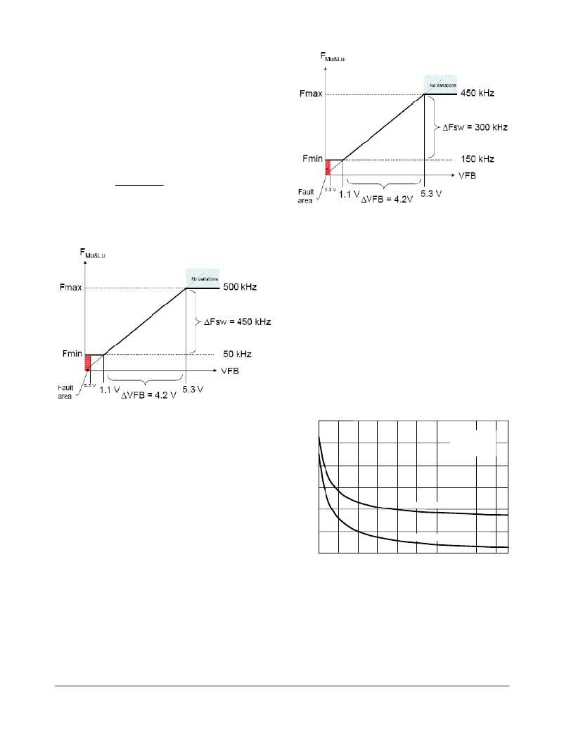
�As� shown� on� Figure� 26,� the� internal� dynamics� of� the� VCO�
�control� voltage� will� be� constrained� between� 0.5� V� and� 2.3� V,�
�whereas� the� feedback� loop� will� drive� Pin� 6� (FB)� between�
�1.1� V� and� 5.3� V.� If� we� take� the� default� FB� pin� excursion�
�numbers,� 1.1� V� =� 50� kHz,� 5.3� V� =� 500� kHz,� then� the� VCO�
�maximum� slope� will� be:�
�500 k� *� 50 k�
�4.2�
�+� 107� kHz/V�
�Figures� 27� and� 28� portray� the� frequency� evolution�
�depending� on� the� feedback� pin� voltage� level� in� a� different�
�frequency� clamp� combination.�
�Figure� 28.� Here� a� different� minimum� frequency� was�
�programmed� as� well� as� a� maximum� frequency�
�excursion�
�Please� note� that� the� previous� small� ?� signal� VCO� slope� has�
�now� been� reduced� to� 300k� /� 4.1� =� 71� kHz� /� V� on� M� upper� and�
�M� lower� outputs.� This� offers� a� mean� to� magnify� the� feedback�
�excursion� on� systems� where� the� load� range� does� not� generate�
�a� wide� switching� frequency� excursion.� Due� to� this� option,�
�we� will� see� how� it� becomes� possible� to� observe� the� feedback�
�level� and� implement� skip� cycle� at� light� loads.� It� is� important�
�to� note� that� the� frequency� evolution� does� not� have� a� real�
�linear� relationship� with� the� feedback� voltage.� This� is� due� to�
�the� deadtime� presence� which� stays� constant� as� the� switching�
�period� changes.�
�The� selection� of� the� three� setting� resistors� (F� max� ,� F� min� and�
�deadtime)� requires� the� usage� of� the� selection� charts�
�displayed� below:�
�Figure� 27.� Maximal� Default� Excursion,�
�Rt� =� 41� k� W� on� Pin� 4� and� R� F(max)� =� 1.9� k� W� on� Pin� 2�
�550�
�450�
�350�
�250�
�150�
�V� CC� =� 15� V�
�V� FB� =� 6.5� V�
�DT� =� 300� ns�
�F� min� = 200 kHz�
�F� min� =� 50� kHz�
�50�
�1.9�
�11.9�
�21.9�
�31.9�
�41.9�
�R� Fmax� (k� W� )�
�Figure� 29.� Maximum� Switching� Frequency� Resistor�
�Selection� Depending� on� the� Adopted� Minimum�
�Switching� Frequency�
�http://onsemi.com�
�14�
�相关PDF资料 |
PDF描述 |
|---|---|
| VI-27N-EY-F2 | CONVERTER MOD DC/DC 18.5V 50W |
| NCP4302ADR2G | IC REG CTRLR FLYBK ISO PWM 8SOIC |
| VI-27M-EY-F4 | CONVERTER MOD DC/DC 10V 50W |
| VI-27M-EY-F2 | CONVERTER MOD DC/DC 10V 50W |
| UC3845BVDG | IC REG CTRLR PWM CM 14-SOIC |
相关代理商/技术参数 |
参数描述 |
|---|---|
| NCP1397DR2G | 制造商:ONSEMI 制造商全称:ON Semiconductor 功能描述:High Performance Resonant Mode Controller with Integrated High-Voltage Drivers |
| NCP1398_13 | 制造商:ONSEMI 制造商全称:ON Semiconductor 功能描述:High Performance Resonant Mode Controller with Integrated High-Voltage Drivers |
| NCP1398B | 制造商:ONSEMI 制造商全称:ON Semiconductor 功能描述:High Performance Resonant Mode Controller with Integrated High-Voltage Drivers |
| NCP1398BDR2G | 功能描述:功率驱动器IC HI-PERF RES MODE CTR W/ H RoHS:否 制造商:Micrel 产品:MOSFET Gate Drivers 类型:Low Cost High or Low Side MOSFET Driver 上升时间: 下降时间: 电源电压-最大:30 V 电源电压-最小:2.75 V 电源电流: 最大功率耗散: 最大工作温度:+ 85 C 安装风格:SMD/SMT 封装 / 箱体:SOIC-8 封装:Tube |
| NCP1398CDR2G | 制造商:ON Semiconductor 功能描述:HI-PERF RES MODE CTR W/ H - Tape and Reel 制造商:ON Semiconductor 功能描述:REEL / HI-PERF RES MODE CTR W/ H |
发布紧急采购,3分钟左右您将得到回复。