- 您现在的位置:买卖IC网 > PDF目录299551 > NCP1546DG (ON SEMICONDUCTOR) 1.5A 170 kHz Low Voltage Buck Regulator PDF资料下载
参数资料
| 型号: | NCP1546DG |
| 厂商: | ON SEMICONDUCTOR |
| 元件分类: | 稳压器 |
| 英文描述: | 1.5A 170 kHz Low Voltage Buck Regulator |
| 中文描述: | SWITCHING REGULATOR, PDSO8 |
| 封装: | LEAD FREE, SOIC-8 |
| 文件页数: | 14/15页 |
| 文件大小: | 212K |
| 代理商: | NCP1546DG |
NCP1546
http://onsemi.com
8
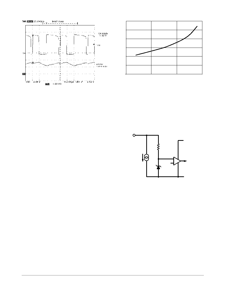
Figure 8. The Regulator in Current Limit
BOOST Pin
The BOOST pin provides base driving current for the
power switch. A voltage higher than VIN provides required
headroom to turn on the power switch. This in turn reduces
IC power dissipation and improves overall system
efficiency. The BOOST pin can be connected to an external
booststrapping circuit which typically uses a 0.1
mF
capacitor and a 1N914 or 1N4148 diode, as shown in Figure
1. When the power switch is turned on, the voltage on the
BOOST pin is equal to
VBOOST + VIN ) VO * VF
where:
VF = diode forward voltage.
The anode of the diode can be connected to any DC
voltage as well as the regulated output voltage (Figure 1).
However, the maximum voltage on the BOOST pin shall not
exceed 40 V.
As shown in Figure 9, the BOOST pin current includes a
constant 7.0 mA predriver current and base current
proportional to switch conducting current. A detailed
discussion of this current is conducted in Thermal
Consideration section. A 0.1
mF capacitor is usually adequate
for maintaining the Boost pin voltage during the on time.
Figure 9. The Boost Pin Current Includes 7.0 mA
PreDriver Current and Base Current when the
Switch is Turned On. The Beta Decline of the
Power Switch Further Increases the Base
Current at High Switching Current
0
0.5
1.0
1.5
SWITCHING CURRENT (A)
BOOST
PIN
CURRENT
(mA)
0
5
10
15
20
25
30
Shutdown
The internal power switch will not turn on until the VIN
pin rises above the Startup Voltage. This ensures no
switching will occur until adequate supply voltage is
provided to the IC. Refer to Figure 10 for the SHDNB
(shutdownbar) pin input circuit.
Figure 10.
+
-
SHDNB
VIN
GND
1.2V
20k
±33%
VZ = 6V to 8V
1
mA
to
10
mA
The IC enters a sleep mode when the SHDNB pin is pulled
below the Shutdown Threshold Voltage. In sleep mode, the
power switch is kept open and the supply current reduces to
Shutdown Quiescent Current ( 1
mA typically). This pin has
an internal pulldown current. When not in use, pull this pin
resistor will ensure safe operation from below 9 V and
during a 40 V load dump condition.
相关PDF资料 |
PDF描述 |
|---|---|
| NCP362BMUTBG | OVP/OCP + TVS |
| NCT1008DMT3R2G | %2B-1℃ temperature monitor with series resistance cancellation |
| NCV4275ADS50G | 450 mA, 5.0V, LDO w/Reset and Delay |
| NCV4275ADS50R4G | 450 mA, 5.0V, LDO w/Reset and Delay |
| NCV4275ADT33RKG | 450 mA, 3.3 V, LDO w/Reset and Delay |
相关代理商/技术参数 |
参数描述 |
|---|---|
| NCP1546DR2G | 功能描述:直流/直流开关调节器 1.5A LOW VOLTAGE REG RoHS:否 制造商:International Rectifier 最大输入电压:21 V 开关频率:1.5 MHz 输出电压:0.5 V to 0.86 V 输出电流:4 A 输出端数量: 最大工作温度: 安装风格:SMD/SMT 封装 / 箱体:PQFN 4 x 5 |
| NCP1546MNR2G | 功能描述:直流/直流开关调节器 170 KHZ RoHS:否 制造商:International Rectifier 最大输入电压:21 V 开关频率:1.5 MHz 输出电压:0.5 V to 0.86 V 输出电流:4 A 输出端数量: 最大工作温度: 安装风格:SMD/SMT 封装 / 箱体:PQFN 4 x 5 |
| NCP1547DG | 功能描述:直流/直流开关调节器 340 KHZ REGULATOR RoHS:否 制造商:International Rectifier 最大输入电压:21 V 开关频率:1.5 MHz 输出电压:0.5 V to 0.86 V 输出电流:4 A 输出端数量: 最大工作温度: 安装风格:SMD/SMT 封装 / 箱体:PQFN 4 x 5 |
| NCP1547DR2G | 功能描述:直流/直流开关调节器 340 KHZ REGULATOR RoHS:否 制造商:International Rectifier 最大输入电压:21 V 开关频率:1.5 MHz 输出电压:0.5 V to 0.86 V 输出电流:4 A 输出端数量: 最大工作温度: 安装风格:SMD/SMT 封装 / 箱体:PQFN 4 x 5 |
| NCP1547MNR2G | 功能描述:直流/直流开关调节器 340 KHZ RoHS:否 制造商:International Rectifier 最大输入电压:21 V 开关频率:1.5 MHz 输出电压:0.5 V to 0.86 V 输出电流:4 A 输出端数量: 最大工作温度: 安装风格:SMD/SMT 封装 / 箱体:PQFN 4 x 5 |
发布紧急采购,3分钟左右您将得到回复。