- 您现在的位置:买卖IC网 > PDF目录15205 > NCP1562ADBR2G (ON Semiconductor)IC REG CTRLR PWM VM 16-TSSOP PDF资料下载
参数资料
| 型号: | NCP1562ADBR2G |
| 厂商: | ON Semiconductor |
| 文件页数: | 17/26页 |
| 文件大小: | 0K |
| 描述: | IC REG CTRLR PWM VM 16-TSSOP |
| 标准包装: | 1 |
| PWM 型: | 电压模式 |
| 输出数: | 2 |
| 频率 - 最大: | 1MHz |
| 占空比: | 85% |
| 电源电压: | 23.2 V ~ 100 V |
| 降压: | 无 |
| 升压: | 是 |
| 回扫: | 是 |
| 反相: | 是 |
| 倍增器: | 无 |
| 除法器: | 无 |
| Cuk: | 无 |
| 隔离: | 无 |
| 工作温度: | -40°C ~ 125°C |
| 封装/外壳: | 16-TSSOP(0.173",4.40mm 宽) |
| 包装: | 剪切带 (CT) |
| 其它名称: | NCP1562ADBR2GOSCT |
�� �
�
�NCP1562A,� NCP1562B�
�In� some� instances� it� may� be� desired� to� latch� (instead� of�
�auto� re--� start)� the� NCP1562� after� a� cycle� skip� event� is�
�detected.� This� can� be� easily� achieved� by� adding� an� external�
�latch.� Figures� 35� and� 36� show� an� implementation� of� an�
�integrated� and� a� discrete� latch,� respectively.� In� general� the�
�circuits� work� by� pulling� CSKIP� to� V� REF� ,� preventing� it� from�
�reaching� V� CSKIP(valley)� once� the� CSKIP� voltage� reaches� the�
�turn� on� threshold� of� the� latch.� The� external� latch� is� cleared�
�by� bringing� the� UVOV� voltage� below� V� UV� and� disabling�
�V� REF� .�
�V� REF�
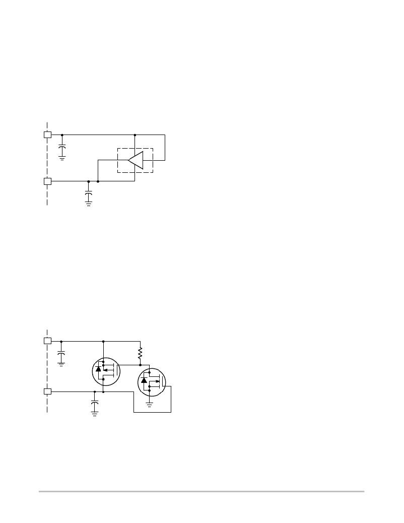
�A� latch� implemented� using� discrete� N� and� P--� channel�
�MOSFETs� is� shown� in� Figure� 39.� The� latch� is� enabled� once�
�the� CSKIP� voltage� reaches� the� threshold� of� M1.� Once� M1�
�turns� on,� it� pulls� low� the� gate� of� M2.� CSKIP� is� then� pulled�
�to� V� REF� by� M2.� It� is� important� to� size� R� pull--up� correctly.� If�
�R� pull--up� is� too� big,� it� will� not� keep� M2� off� while� V� REF�
�charges.� This� will� cause� the� controller� to� latch� during� initial�
�power--� up.� In� this� particular� implementation� the� turn� on�
�threshold� of� M1� is� 2� V� and� R� pull--up� is� sized� to� 24.9� k� ?� .�
�Leading� Edge� Blanking�
�The� current� sense� signal� is� prone� to� leading� edge� spikes�
�caused� by� the� power� switch� transitions.� The� current� signal�
�C� REF�
�OUTY�
�V� CC�
�INA�
�is� usually� filtered� using� an� RC� low–pass� filter� to� avoid�
�premature� triggering� of� the� current� limit� circuit.� However,�
�the� low� pass� filter� will� inevitably� change� the� shape� of� the�
�current� pulse� and� also� add� cost� and� complexity.� The�
�CSKIP�
�OE�
�MC74VHC1GT126�
�NCP1562� uses� LEB� circuitry� that� blocks� out� the� first� 70� ns�
�(typ)� of� each� current� pulse.� This� removes� the� leading� edge�
�spikes� without� altering� the� current� waveform.� The� blanking�
�C� CSKIP�
�Figure� 38.� External� Latch� Implemented� using�
�ON� Semiconductor’s� MiniGate� t� Buffer�
�The� latch� in� Figure� 38� consists� of� a� TTL� level� tri--� state�
�output� buffer� from� ON� Semiconductor� ’s� MiniGate� t�
�family.� The� enable� (OE)� and� output� (OUTY)� terminals� are�
�connected� to� CSKIP� and� the� V� CC� and� INA� pins� are�
�connected� to� V� REF� .� The� output� of� the� buffer� is� in� a� high�
�impedance� mode� when� OE� is� low.� Once� a� continuous�
�current� limit� condition� is� detected,� the� CSKIP� timer� is�
�enabled� and� CSKIP� begins� charging.� Once� the� voltage� on�
�CSKIP� reaches� the� enable� threshold� of� the� buffer,� the�
�output� of� the� buffer� is� pulled� to� V� REF� ,� latching� the� CSKIP�
�timer.� The� OE� threshold� of� the� buffer� is� typically� 1.5� V.�
�period� is� disabled� during� soft--� start� as� the� blanking� period�
�may� be� longer� than� the� startup� duty� cycle.� It� is� also� disabled�
�if� the� output� of� the� Saturation� Comparator� is� low,� indicating�
�that� the� output� is� not� yet� in� regulation.� This� occurs� during�
�power� up� or� during� an� output� overload� condition.�
�Supply� Voltage� and� Startup� Circuit�
�The� NCP1562� internal� startup� regulator� eliminates� the�
�need� for� external� startup� components.� In� addition,� this�
�regulator� increases� the� efficiency� of� the� supply� as� it� uses� no�
�power� when� in� the� normal� mode� of� operation,� but� instead�
�uses� power� supplied� by� an� auxiliary� winding.� The�
�NCP1562� incorporates� an� optimized� startup� circuit� that�
�reduces� the� requirement� of� the� supply� capacitor,�
�particularly� important� in� size� constrained� applications.�
�The� startup� regulator� consists� of� a� constant� current�
�source� that� supplies� current� from� the� input� line� voltage�
�V� REF�
�C� REF� BSS84L�
�24.9� k� Ω�
�R� pull--up�
�(V� in� )� to� the� supply� capacitor� on� the� V� AUX� pin� (C� AUX� ).� The�
�startup� current� (I� start� )� is� typically� 10� mA.�
�Once� C� AUX� is� charged� to� 10.3� V� (V� AUX(on)� ),� the� startup�
�regulator� is� disabled� and� the� outputs� are� enabled� if� there� are�
�no� UV,� OV,� cycle� skip� or� thermal� shutdown� faults.� The�
�CSKIP�
�M2�
�C� CSKIP�
�M1�
�2N7002L�
�startup� regulator� remains� disabled� until� the� lower� voltage�
�threshold� (V� AUX(off1)� )� of� 8.0� V� is� reached.� Once� reached,�
�the� startup� circuit� is� enabled.� If� the� bias� current� requirement�
�out� of� C� AUX� is� greater� than� the� startup� current,� V� AUX� will�
�discharge� until� reaching� the� lower� voltage� threshold�
�(V� AUX(off2)� )� of� 7.0� V.� Upon� reaching� V� AUX(off2)� ,� the�
�outputs� are� disabled.� Once� the� outputs� are� disabled,� the� bias�
�Figure� 39.� External� Latch� Implemented� using�
�Discrete� N� and� P--Channel� MOSFETs�
�current� of� the� IC� is� reduced,� allowing� V� AUX� to� charge� back�
�up.� This� mode� of� operation� allows� a� dramatic� reduction� in�
�the� size� of� C� AUX� as� not� all� the� power� required� for� startup�
�needs� to� be� stored� by� C� AUX� .� This� mode� of� operation� is�
�known� as� Dynamic� Self� Supply� (DSS).� Figure� 40� shows� the�
�relationship� between� V� AUX(on)� ,� V� AUX(off1)� ,� V� AUX(off2)� and�
�UV.� As� shown� in� Figure� 40,� the� outputs� are� not� enabled�
�until� the� UV� fault� is� removed� and� V� AUX� reaches� V� AUX(on)� .�
�http://onsemi.com�
�17�
�相关PDF资料 |
PDF描述 |
|---|---|
| NCV303LSN20T1G | IC VOLT DETECTOR 2.0V TSOP-5 |
| GEC60DRTH-S93 | CONN EDGECARD 120PS DIP .100 SLD |
| NCV303LSN16T1G | IC VOLT DETECTOR 1.6V TSOP-5 |
| H2AAT-10106-R4-ND | JUMPER-H1502TR/A2015R/H1502TR 6" |
| H2AAT-10106-N4-ND | JUMPER-H1502TR/A2015N/H1502TR 6" |
相关代理商/技术参数 |
参数描述 |
|---|---|
| NCP1562ADR2G | 功能描述:电压模式 PWM 控制器 HI PERF RESET PWM CONTLR RoHS:否 制造商:Texas Instruments 输出端数量:1 拓扑结构:Buck 输出电压:34 V 输出电流: 开关频率: 工作电源电压:4.5 V to 5.5 V 电源电流:600 uA 最大工作温度:+ 125 C 最小工作温度:- 40 C 封装 / 箱体:WSON-8 封装:Reel |
| NCP1562BDBR2G | 功能描述:电压模式 PWM 控制器 HI PERF RESET PWM CONTLR RoHS:否 制造商:Texas Instruments 输出端数量:1 拓扑结构:Buck 输出电压:34 V 输出电流: 开关频率: 工作电源电压:4.5 V to 5.5 V 电源电流:600 uA 最大工作温度:+ 125 C 最小工作温度:- 40 C 封装 / 箱体:WSON-8 封装:Reel |
| NCP1562BDR2G | 功能描述:电压模式 PWM 控制器 HI PERF RESET PWM CONTLR RoHS:否 制造商:Texas Instruments 输出端数量:1 拓扑结构:Buck 输出电压:34 V 输出电流: 开关频率: 工作电源电压:4.5 V to 5.5 V 电源电流:600 uA 最大工作温度:+ 125 C 最小工作温度:- 40 C 封装 / 箱体:WSON-8 封装:Reel |
| NCP1571D | 功能描述:DC/DC 开关控制器 Low Voltage RoHS:否 制造商:Texas Instruments 输入电压:6 V to 100 V 开关频率: 输出电压:1.215 V to 80 V 输出电流:3.5 A 输出端数量:1 最大工作温度:+ 125 C 安装风格: 封装 / 箱体:CPAK |
| NCP1571DG | 功能描述:DC/DC 开关控制器 Low Voltage Synchronous Buck RoHS:否 制造商:Texas Instruments 输入电压:6 V to 100 V 开关频率: 输出电压:1.215 V to 80 V 输出电流:3.5 A 输出端数量:1 最大工作温度:+ 125 C 安装风格: 封装 / 箱体:CPAK |
发布紧急采购,3分钟左右您将得到回复。