- 您现在的位置:买卖IC网 > PDF目录15205 > NCP1562BDBR2G (ON Semiconductor)IC REG CTRLR PWM VM 16-TSSOP PDF资料下载
参数资料
| 型号: | NCP1562BDBR2G |
| 厂商: | ON Semiconductor |
| 文件页数: | 3/26页 |
| 文件大小: | 0K |
| 描述: | IC REG CTRLR PWM VM 16-TSSOP |
| 标准包装: | 1 |
| PWM 型: | 电压模式 |
| 输出数: | 2 |
| 频率 - 最大: | 1MHz |
| 占空比: | 85% |
| 电源电压: | 23.2 V ~ 100 V |
| 降压: | 无 |
| 升压: | 是 |
| 回扫: | 是 |
| 反相: | 是 |
| 倍增器: | 无 |
| 除法器: | 无 |
| Cuk: | 无 |
| 隔离: | 无 |
| 工作温度: | -40°C ~ 125°C |
| 封装/外壳: | 16-TSSOP(0.173",4.40mm 宽) |
| 包装: | 剪切带 (CT) |
| 其它名称: | NCP1562BDBR2GOSCT |
��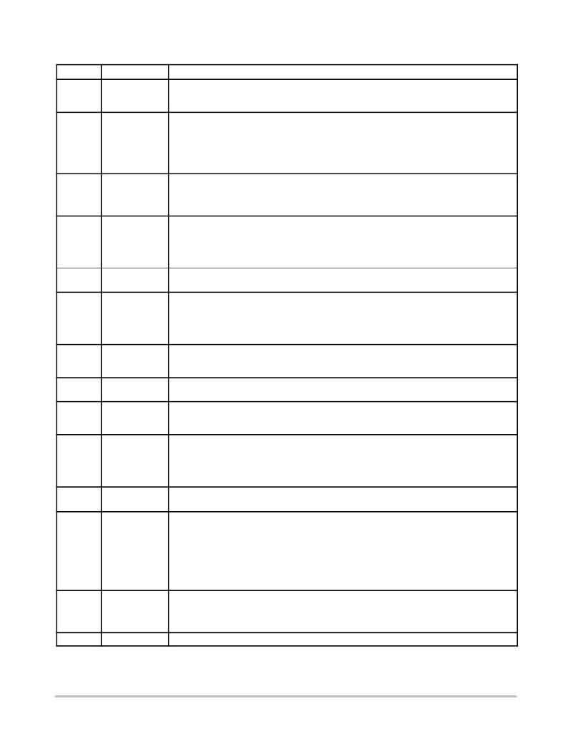 �
�
�NCP1562A,� NCP1562B�
�PIN� FUNCTION� DESCRIPTION�
�Pin�
�1�
�2�
�3�
�4�
�5�
�6�
�7�
�8�
�9�
�10�
�11�
�12�
�13�
�14�
�Symbol�
�V� in�
�UVOV�
�FF�
�CS�
�GND�
�R� T� C� T�
�SYNC�
�V� REF�
�V� EA�
�SS�
�t� D�
�CSKIP�
�OUT2�
�PGND�
�Description�
�Connect� the� input� line� voltage� directly� to� this� pin� to� enable� the� internal� startup� regulator.� A� constant�
�current� source� supplies� current� from� this� pin� to� the� capacitor� connected� to� the� V� AUX� pin,� eliminating� the�
�need� for� a� startup� resistor.� The� charge� current� is� typically� 10� mA.� Maximum� input� voltage� is� 100� V.�
�Input� supply� voltage� is� scaled� down� and� sampled� by� means� of� a� resistor� divider.� The� same� pin� is� used�
�for� both� undervoltage� (UV)� and� overvoltage� (OV)� detection� using� a� novel� architecture� (patent� pending).�
�The� minimum� and� maximum� input� supply� voltage� thresholds� are� adjusted� independently.� A� UV�
�condition� exists� if� the� UVOV� voltage� is� below� 2.0� V� and� an� OV� condition� exists� if� the� UVOV� voltage�
�exceeds� 3.0� V.� The� undervoltage� threshold� is� trimmed� during� manufacturing� to� obtain� ?� 3%� accuracy�
�allowing� a� tighter� power� stage� design.� Both� the� UV� and� OV� detectors� have� a� 100� mV� hysteresis.�
�An� external� R--C� divider� from� the� input� line� generates� the� Feedforward� Ramp.� This� ramp� is� used� by� the�
�PWM� comparator� to� set� the� duty� cycle,� thus� providing� direct� line� regulation.� An� internal� pulldown�
�transistor� discharges� the� external� capacitor� every� cycle.� Once� discharged,� the� capacitor� is� effectively�
�grounded� until� the� next� cycle� begins.�
�Overcurrent� sense� input.� If� the� CS� voltage� exceeds� 0.2� V� (or� 0.5� V� in� the� NCP1562B)� the� converter�
�operates� in� cycle--by--cycle� current� limit.� Once� a� current� limit� pulse� is� detected,� the� cycle� skip� timer� is�
�enabled.� Internal� leading� edge� blanking� pulse� prevents� nuisance� triggering� during� normal� operation.�
�The� leading� edge� blanking� is� disabled� during� soft--start� and� output� overload� conditions� to� improve� the�
�response� to� faults.�
�Control� circuit� ground.� All� control� and� timing� components� that� connect� to� GND� should� have� the� shortest�
�loop� possible� to� this� pin� to� improve� noise� immunity.�
�An� external� R� T� --C� T� divider� from� V� REF� sets� the� operating� frequency� and� maximum� duty� cycle� of� OUT1.�
�The� maximum� operating� frequency� is� 1.0� MHz.� A� sawtooth� Ramp� between� 2.0� V� and� 3.0� V� is�
�generated� by� sequentially� charging� and� discharging� C� T� .� The� peak� and� valley� of� the� Ramp� are�
�accurately� controlled� to� provide� precise� control� of� the� duty� cycle� and� frequency.� The� outputs� are�
�disabled� during� the� C� T� discharge� time.�
�Proprietary� bidirectional� frequency� synchronization� architecture� allows� two� NCP1562� devices� to�
�synchronize� together.� The� lower� frequency� device� becomes� the� slave.� It� can� also� synchronize� to� an�
�external� signal.�
�Precision� 5.0� V� reference.� Maximum� output� current� is� 5.0� mA.� It� is� required� to� bypass� the� reference�
�with� a� capacitor.� The� recommended� capacitance� range� is� between� 0.047� m� F� and� 1.0� m� F.�
�The� error� signal� from� an� external� error� amplifier� is� fed� to� this� input� and� compared� to� the� Feedforward�
�Ramp.� A� series� diode� and� resistor� offset� the� voltage� on� this� pin� before� it� is� applied� to� the� PWM�
�Comparator� inverting� input.� An� internal� pullup� resistor� allows� direct� connection� to� an� optocoupler.�
�A� 10� m� A� current� source� charges� the� external� capacitor� connected� to� this� pin.� Duty� cycle� is� limited�
�during� startup� by� comparing� the� voltage� on� this� pin� to� the� Feedforward� Ramp.� Under� steady� state�
�conditions,� the� SS� voltage� is� approximately� 3.8� V.� Once� a� UV,� OV,� overtemperature� or� cycle� skip� fault�
�is� detected,� the� SS� capacitor� is� discharged� in� a� controlled� manner� with� a� 100� m� A� current� source.� The�
�duty� cycle� is� then� slowly� reduced� until� reaching� 0%.�
�An� external� resistor� between� this� pin� and� GND� sets� the� overlap� time� delay� between� OUT1� and� OUT2�
�transitions.�
�The� converter� is� disabled� if� a� continuous� overcurrent� condition� exists.� The� time� to� determine� the� fault�
�and� the� time� the� converter� is� disabled� are� programmed� by� the� capacitor� (C� CSKIP� )� connected� to� this� pin.�
�The� cycle� skip� timer� is� enabled� after� a� current� limit� fault� is� detected.� Once� enabled,� C� CSKIP� is� charged�
�with� a� 100� m� A� source.� If� the� overcurrent� fault� is� removed� before� entering� the� soft--stop� mode,� the�
�capacitor� is� discharged� with� a� 10� m� A� source.� Once� C� CSKIP� reaches� 3.0� V,� the� converter� enters� a�
�soft--stop� mode� and� C� CSKIP� is� discharged� with� a� 10� m� A� source.� The� converter� is� re--enabled� once�
�C� CSKIP� reaches� 0.5� V.� If� the� condition� resulting� in� overcurrent� is� cleared� during� this� phase,� C� CSKIP�
�discharges� to� 0� V.� Otherwise,� it� starts� charging� from� 0.5� V,� setting� up� a� hiccup� mode� operation.�
�Secondary� output� of� the� PWM� Controller.� It� can� be� used� to� drive� an� active� clamp/reset� switch,� a�
�synchronous� rectifier� topology,� or� both.� OUT2� has� an� adjustable� leading� and� trailing� edge� overlap� delay�
�against� OUT1.� OUT2� has� source� and� sink� resistances� of� 12� Ω� (typ.).� OUT2� is� designed� to� handle� up�
�to� 1.0� A.�
�Ground� connection� for� OUT1� and� OUT2.� Tie� to� the� power� stage� return� with� a� short� loop.�
�http://onsemi.com�
�3�
�相关PDF资料 |
PDF描述 |
|---|---|
| VI-J54-EY-F1 | CONVERTER MOD DC/DC 48V 50W |
| VE-B4N-EV-F2 | CONVERTER MOD DC/DC 18.5V 150W |
| VI-B7Z-EY-F4 | CONVERTER MOD DC/DC 2V 20W |
| GEC60DRTN-S93 | CONN EDGECARD 120PS DIP .100 SLD |
| VI-B7Z-EY-F3 | CONVERTER MOD DC/DC 2V 20W |
相关代理商/技术参数 |
参数描述 |
|---|---|
| NCP1562BDR2G | 功能描述:电压模式 PWM 控制器 HI PERF RESET PWM CONTLR RoHS:否 制造商:Texas Instruments 输出端数量:1 拓扑结构:Buck 输出电压:34 V 输出电流: 开关频率: 工作电源电压:4.5 V to 5.5 V 电源电流:600 uA 最大工作温度:+ 125 C 最小工作温度:- 40 C 封装 / 箱体:WSON-8 封装:Reel |
| NCP1571D | 功能描述:DC/DC 开关控制器 Low Voltage RoHS:否 制造商:Texas Instruments 输入电压:6 V to 100 V 开关频率: 输出电压:1.215 V to 80 V 输出电流:3.5 A 输出端数量:1 最大工作温度:+ 125 C 安装风格: 封装 / 箱体:CPAK |
| NCP1571DG | 功能描述:DC/DC 开关控制器 Low Voltage Synchronous Buck RoHS:否 制造商:Texas Instruments 输入电压:6 V to 100 V 开关频率: 输出电压:1.215 V to 80 V 输出电流:3.5 A 输出端数量:1 最大工作温度:+ 125 C 安装风格: 封装 / 箱体:CPAK |
| NCP1571DR2 | 功能描述:DC/DC 开关控制器 Low Voltage RoHS:否 制造商:Texas Instruments 输入电压:6 V to 100 V 开关频率: 输出电压:1.215 V to 80 V 输出电流:3.5 A 输出端数量:1 最大工作温度:+ 125 C 安装风格: 封装 / 箱体:CPAK |
| NCP1571DR2G | 功能描述:DC/DC 开关控制器 Low Voltage Synchronous Buck RoHS:否 制造商:Texas Instruments 输入电压:6 V to 100 V 开关频率: 输出电压:1.215 V to 80 V 输出电流:3.5 A 输出端数量:1 最大工作温度:+ 125 C 安装风格: 封装 / 箱体:CPAK |
发布紧急采购,3分钟左右您将得到回复。