- 您现在的位置:买卖IC网 > Datasheet目录45 > NCP1578MNR2G (ON Semiconductor)IC REG DL BCK/LINEAR SYNC 20-QFN Datasheet资料下载
参数资料
| 型号: | NCP1578MNR2G |
| 厂商: | ON Semiconductor |
| 文件页数: | 4/22页 |
| 文件大小: | 1861K |
| 描述: | IC REG DL BCK/LINEAR SYNC 20-QFN |
| 产品变化通告: | Product Obsolescence 19/Dec/2008 |
| 标准包装: | 4,000 |
| 拓扑: | 降压(降压)同步(1),线性(LDO)(1) |
| 功能: | 任何功能 |
| 输出数: | 2 |
| 频率 - 开关: | 300kHz |
| 电压/电流 - 输出 1: | 控制器 |
| 电压/电流 - 输出 2: | 5V,50mA |
| 带 LED 驱动器: | 无 |
| 带监控器: | 无 |
| 带序列发生器: | 是 |
| 电源电压: | 4.5 V ~ 24 V |
| 工作温度: | -40°C ~ 85°C |
| 安装类型: | 表面贴装 |
| 封装/外壳: | 20-VFQFN 裸露焊盘 |
| 供应商设备封装: | 20-QFN(4x4) |
| 包装: | 带卷 (TR) |
NCP1578
http://onsemi.com
4
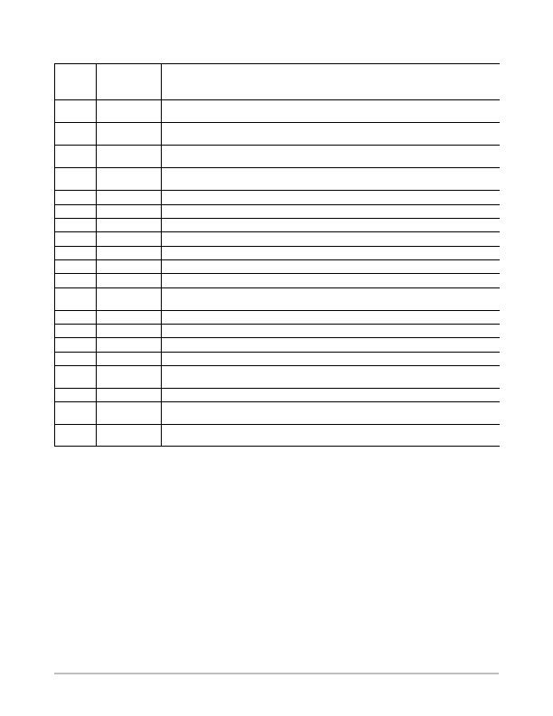
PIN FUNCTION DESCRIPTION
Pin No.
Symbol
Description
1
FPWM
FPWM or Power Saving Control. Logic high enables force PWM. Logic low enables power saving
operation.
2
EN_LDO
LDO enable input. The 5 V LDO is enabled if EN_LDO is high and disabled if it is low. This pin can
sustain voltage as high as VBAT.
3
OCSET
Input pin for over current threshold setting for high side gate driver. Also it is for the internal ramp gen
erator to implement the voltage feed forward rejection to the input voltage variation
4
FOFF
Fault OFF. If it pulls to high, it disables the features of OCP, UVLO and OVP. Normally it should be tied
to ground. This pin is internally pulled down.
5
EN_SW
PWM controller's enable input. The switching controller is enabled if EN_SW is high and disabled if
EN is low.
6
LDO5
5.0 V linear regulator output.
7
VBAT
Battery/adaptor voltage input.
8
AGND
Analog ground.
9
NC
Not connected
10
FB
Feedback input from controller's output voltage.
11
COMP
Error amplifier output pin.
12
SS
Soft-start (for switcher) capacitor connection to ground.
13
PGOOD
Power good signal open drain output. High impedance (open drain) if power is good (in regulation).
Low impedance if power is not good.
14
PGDLY
Power good delay capacitor connection to ground.
15
PGND
Power ground.
16
BG
Gate driver output for low-side N-Channel power FET.
17
VCCP
Power Input voltage pin.
18
SWN
Inductor driven node of the SMPS, the return for high-side gate driver, and also serve as the lower
supply rail of the high-side gate driver of the SMPS.
19
TG
Gate driver output for high-side N-Channel power FET.
20
VBST
Positive supply of high-side gate driver of the SMPS. Connect boost capacitor between this pin and
switching node SWN of the SMPS.
21
THPAD
Copper pad on bottom of IC used for heatsinking. This pin should be connected to the ground plane
under the IC.
相关PDF资料 |
PDF描述 |
|---|---|
| NCP1601BDR2G | IC PFC CTRL CRM/TRANSITION 8SOIC |
| NCP1603D100R2G | IC CTLR PFC/PWM COMBO 16-SOIC |
| NCP1605DR2G | IC PFC CONTROLLER CCM/DCM 16SOIC |
| NCP1606BDR2G | IC POWER FACTOR CONTROLLER 8SOIC |
| NCP1607BDR2G | IC PFC CONTROLLER CRM 8SOIC |
相关代理商/技术参数 |
参数描述 |
|---|---|
| NCP1579DR2G | 功能描述:电压模式 PWM 控制器 BUCK CONTROLLER RoHS:否 制造商:Texas Instruments 输出端数量:1 拓扑结构:Buck 输出电压:34 V 输出电流: 开关频率: 工作电源电压:4.5 V to 5.5 V 电源电流:600 uA 最大工作温度:+ 125 C 最小工作温度:- 40 C 封装 / 箱体:WSON-8 封装:Reel |
| NCP1580DR2 | 功能描述:电压模式 PWM 控制器 Low Voltage RoHS:否 制造商:Texas Instruments 输出端数量:1 拓扑结构:Buck 输出电压:34 V 输出电流: 开关频率: 工作电源电压:4.5 V to 5.5 V 电源电流:600 uA 最大工作温度:+ 125 C 最小工作温度:- 40 C 封装 / 箱体:WSON-8 封装:Reel |
| NCP1580DR2G | 功能描述:电压模式 PWM 控制器 Low Voltage Synchronous Buck RoHS:否 制造商:Texas Instruments 输出端数量:1 拓扑结构:Buck 输出电压:34 V 输出电流: 开关频率: 工作电源电压:4.5 V to 5.5 V 电源电流:600 uA 最大工作温度:+ 125 C 最小工作温度:- 40 C 封装 / 箱体:WSON-8 封装:Reel |
| NCP1581DR2G | 功能描述:电压模式 PWM 控制器 SYNCHRONOUS PWM BUCK CONV RoHS:否 制造商:Texas Instruments 输出端数量:1 拓扑结构:Buck 输出电压:34 V 输出电流: 开关频率: 工作电源电压:4.5 V to 5.5 V 电源电流:600 uA 最大工作温度:+ 125 C 最小工作温度:- 40 C 封装 / 箱体:WSON-8 封装:Reel |
| NCP1581SBCKRGEVB | 功能描述:BOARD EVAL NCP1581 RoHS:是 类别:编程器,开发系统 >> 评估板 - DC/DC 与 AC/DC(离线)SMPS 系列:* 产品培训模块:Obsolescence Mitigation Program 标准包装:1 系列:True Shutdown™ 主要目的:DC/DC,步升 输出及类型:1,非隔离 功率 - 输出:- 输出电压:- 电流 - 输出:1A 输入电压:2.5 V ~ 5.5 V 稳压器拓扑结构:升压 频率 - 开关:3MHz 板类型:完全填充 已供物品:板 已用 IC / 零件:MAX8969 |
发布紧急采购,3分钟左右您将得到回复。