- 您现在的位置:买卖IC网 > PDF目录15054 > NCP1582DR2G (ON Semiconductor)IC REG CTRLR BUCK PWM VM 8-SOIC PDF资料下载
参数资料
| 型号: | NCP1582DR2G |
| 厂商: | ON Semiconductor |
| 文件页数: | 3/16页 |
| 文件大小: | 0K |
| 描述: | IC REG CTRLR BUCK PWM VM 8-SOIC |
| 产品变化通告: | Product Discontinuation 01/Oct/2008 |
| 标准包装: | 2,500 |
| PWM 型: | 电压模式 |
| 输出数: | 1 |
| 频率 - 最大: | 400kHz |
| 占空比: | 80% |
| 电源电压: | 4.5 V ~ 13.2 V |
| 降压: | 是 |
| 升压: | 无 |
| 回扫: | 无 |
| 反相: | 无 |
| 倍增器: | 无 |
| 除法器: | 无 |
| Cuk: | 无 |
| 隔离: | 无 |
| 工作温度: | 0°C ~ 70°C |
| 封装/外壳: | 8-SOIC(0.154",3.90mm 宽) |
| 包装: | 带卷 (TR) |
�� �
�
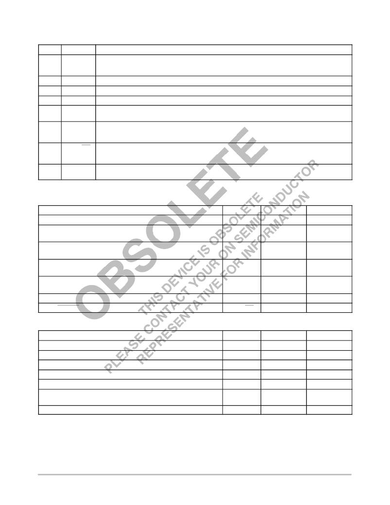
�NCP1582,� NCP1582A,� NCP1583�
�PIN� FUNCTION� DESCRIPTION�
�Pin� No.�
�1�
�2�
�3�
�4�
�5�
�6�
�7�
�8�
�Symbol�
�BST�
�TG�
�GND�
�BG�
�V� CC�
�FB�
�COMP/DIS�
�PHASE�
�Description�
�Supply� rail� for� the� floating� top� gate� driver.� To� form� a� boost� circuit,� use� an� external� diode� to� bring� the�
�desired� input� voltage� to� this� pin� (cathode� connected� to� BST� pin).� Connect� a� capacitor� (C� BST� )� between� this� pin�
�and� the� PHASE� pin.� Typical� values� for� C� BST� range� from� 0.1� m� F� to� 1� m� F.� Ensure� that� C� BST� is� placed� near� the� IC.�
�Top� gate� MOSFET� driver� pin.� Connect� this� pin� to� the� gate� of� the� top� N� ?� Channel� MOSFET.�
�IC� ground� reference.� All� control� circuits� are� referenced� to� this� pin.�
�Bottom� gate� MOSFET� driver� pin.� Connect� this� pin� to� the� gate� of� the� bottom� N� ?� Channel� MOSFET.�
�Supply� rail� for� the� internal� circuitry.� Operating� supply� range� is� 4.5� V� to� 15� V.� Decouple� with� a� 1� m� F�
�capacitor� to� GND.� Ensure� that� this� decoupling� capacitor� is� placed� near� the� IC.�
�This� pin� is� the� inverting� input� to� the� error� amplifier.� Use� this� pin� in� conjunction� with� the� COMP� pin� to�
�compensate� the� voltage� ?� control� feedback� loop.� Connect� this� pin� to� the� output� resistor� divider� (if� used)� or� dir-�
�ectly� to� Vout.�
�Compensation� Pin.� This� is� the� output� of� the� error� amplifier� (EA)� and� the� non� ?� inverting� input� of� the� PWM� com-�
�parator.� Use� this� pin� in� conjunction� with� the� FB� pin� to� compensate� the� voltage� ?� control� feedback� loop.� The� com-�
�pensation� capacitor� also� acts� as� a� soft� ?� start� capacitor.� Pull� this� pin� low� with� an� open� drain� transistor� for� disable.�
�Switch� node� pin.� This� is� the� reference� for� the� floating� top� gate� driver.� Connect� this� pin� to� the� source� of� the� top�
�MOSFET.�
�ABSOLUTE� MAXIMUM� RATINGS�
�Main� Supply� Voltage� Input�
�Bootstrap� Supply� Voltage� Input�
�Pin� Name�
�Symbol�
�V� CC�
�BST�
�V� MAX�
�15� V�
�30� V� wrt/GND�
�V� MIN�
�?� 0.3� V�
�?� 0.3� V�
�15� V� wrt/PHASE�
�Switching� Node� (Bootstrap� Supply� Return)�
�PHASE�
�24� V�
�?� 0.7� V�
�?� 5� V� for� <� 50� ns�
�High� ?� Side� Driver� Output� (Top� Gate)�
�Low� ?� Side� Driver� Output� (Bottom� Gate)�
�TG�
�BG�
�30� V� wrt/GND�
�15� V� wrt/PHASE�
�15� V�
�?� 0.3� V�
�wrt/PHASE�
�?� 0.3� V�
�?� 2� V� for� <� 200� ns�
�Feedback�
�COMP/DISABLE�
�FB�
�COMP/DIS�
�5.5� V�
�5.5� V�
�?� 0.3� V�
�?� 0.3� V�
�MAXIMUM� RATINGS�
�Rating�
�Thermal� Resistance,� Junction� ?� to� ?� Ambient�
�Thermal� Resistance,� Junction� ?� to� ?� Case�
�Operating� Junction� Temperature� Range�
�Operating� Ambient� Temperature� Range�
�Storage� Temperature� Range�
�Lead� Temperature� Soldering� (10� sec):� Reflow� (SMD� styles� only)�
�(Note� 1)�
�Moisture� Sensitivity� Level�
�Pb� ?� Free�
�Symbol�
�R� q� JA�
�R� q� JC�
�T� J�
�T� A�
�T� stg�
�MSL�
�Value�
�165�
�45�
�?� 40� to� 150�
�?� 40� to� 85�
�?� 55� to� +150�
�260� peak�
�1�
�Unit�
�°� C/W�
�°� C/W�
�°� C�
�°� C�
�°� C�
�°� C�
�?�
�Stresses� exceeding� Maximum� Ratings� may� damage� the� device.� Maximum� Ratings� are� stress� ratings� only.� Functional� operation� above� the�
�Recommended� Operating� Conditions� is� not� implied.� Extended� exposure� to� stresses� above� the� Recommended� Operating� Conditions� may� affect�
�device� reliability.�
�1.� 60� ?� 180� seconds� minimum� above� 237� °� C.�
�http://onsemi.com�
�3�
�相关PDF资料 |
PDF描述 |
|---|---|
| ASM12DSEH-S243 | CONN EDGECARD 24POS .156 EYELET |
| RCM31DCCT-S189 | CONN EDGECARD 62POS R/A .156 SLD |
| RCM31DCBT-S189 | CONN EDGECARD 62POS R/A .156 SLD |
| RCM31DCAT-S189 | CONN EDGECARD 62POS R/A .156 SLD |
| EYM28DTBT-S189 | CONN EDGECARD 56POS R/A .156 SLD |
相关代理商/技术参数 |
参数描述 |
|---|---|
| NCP1582DR2GEVB | 功能描述:电源管理IC开发工具 ANA SWITCH REG EVAL BOARD RoHS:否 制造商:Maxim Integrated 产品:Evaluation Kits 类型:Battery Management 工具用于评估:MAX17710GB 输入电压: 输出电压:1.8 V |
| NCP1583DR2G | 功能描述:电压模式 PWM 控制器 BUCK CONTROLLER RoHS:否 制造商:Texas Instruments 输出端数量:1 拓扑结构:Buck 输出电压:34 V 输出电流: 开关频率: 工作电源电压:4.5 V to 5.5 V 电源电流:600 uA 最大工作温度:+ 125 C 最小工作温度:- 40 C 封装 / 箱体:WSON-8 封装:Reel |
| NCP1583DR2GEVB | 功能描述:电源管理IC开发工具 ANA SWITCH REG EVAL BOARD RoHS:否 制造商:Maxim Integrated 产品:Evaluation Kits 类型:Battery Management 工具用于评估:MAX17710GB 输入电压: 输出电压:1.8 V |
| NCP1586DR2G | 功能描述:IC REG CTRLR BUCK PWM VM 8-SOIC RoHS:是 类别:集成电路 (IC) >> PMIC - 稳压器 - DC DC 切换控制器 系列:- 标准包装:2,500 系列:- PWM 型:电流模式 输出数:1 频率 - 最大:500kHz 占空比:100% 电源电压:8.2 V ~ 30 V 降压:无 升压:无 回扫:是 反相:无 倍增器:无 除法器:无 Cuk:无 隔离:是 工作温度:0°C ~ 70°C 封装/外壳:8-DIP(0.300",7.62mm) 包装:管件 产品目录页面:1316 (CN2011-ZH PDF) |
| NCP1586DR2GH | 制造商:ON Semiconductor 功能描述: |
发布紧急采购,3分钟左右您将得到回复。