- 您现在的位置:买卖IC网 > PDF目录13310 > NCP1595MNT2G (ON Semiconductor)IC REG BUCK SYNC ADJ 1.5A 6DFN PDF资料下载
参数资料
| 型号: | NCP1595MNT2G |
| 厂商: | ON Semiconductor |
| 文件页数: | 11/13页 |
| 文件大小: | 0K |
| 描述: | IC REG BUCK SYNC ADJ 1.5A 6DFN |
| 标准包装: | 3,000 |
| 类型: | 降压(降压) |
| 输出类型: | 可调式 |
| 输出数: | 1 |
| 输出电压: | 可调至 0.8V |
| 输入电压: | 4 V ~ 5.5 V |
| PWM 型: | 电流模式 |
| 频率 - 开关: | 1MHz |
| 电流 - 输出: | 1.5A |
| 同步整流器: | 是 |
| 工作温度: | -40°C ~ 85°C |
| 安装类型: | 表面贴装 |
| 封装/外壳: | 6-VDFN 裸露焊盘 |
| 包装: | 带卷 (TR) |
| 供应商设备封装: | 6-DFN(3x3) |
�� �
�
�NCP1595,� NCP1595A,� NCP1595C�
�APPLICATION� INFORMATION�
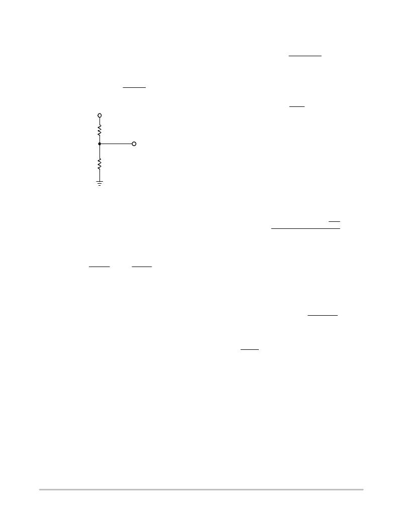
�Programming� the� Output� Voltage�
�The� output� voltage� is� set� using� a� resistive� voltage� divider�
�from� the� output� voltage� to� FB� pin� (see� Figure� 25).� So� the�
�C� OUT(min)� +�
�I� ripple�
�8� @� f� @� V� ripple�
�(eq.� 3)�
�V� out� +� V� FB� @�
�output� voltage� is� calculated� according� to� Eq.1.�
�R� 1� )� R� 2�
�R� 2�
�V� out�
�R1�
�FB�
�R2�
�Figure� 25.� Output� divider�
�(eq.� 1)�
�Where� V� ripple� is� the� allowed� output� voltage� ripple.�
�The� required� ESR� for� this� amount� of� ripple� can� be�
�calculated� by� equation� 5.�
�V� ripple�
�ESR� +� (eq.� 4)�
�I� ripple�
�Based� on� Equation� 2� to� choose� capacitor� and� check� its�
�ESR� according� to� Equation� 3.� If� ESR� exceeds� the� value� from�
�Eq.4,� multiple� capacitors� should� be� used� in� parallel.�
�Ceramic� capacitor� can� be� used� in� most� of� the� applications.�
�In� addition,� both� surface� mount� tantalum� and� through� ?� hole�
�aluminum� electrolytic� capacitors� can� be� used� as� well.�
�Maximum� Output� Capacitor�
�NCP1595/A/C� family� has� internal� 1� ms� fixed� soft� ?� start�
�and� overcurrent� limit.� It� limits� the� maximum� allowed� output�
�capacitor� to� startup� successfully.� The� maximum� allowed�
�output� capacitor� can� be� determined� by� the� equation:�
�C� out(max)� +�
�C� in(min)� +� I� out(max)� @� D� max� @�
�f� @� V� in(ripple)�
�Inductor� Selection�
�The� inductor� is� the� key� component� in� the� switching�
�regulator.� The� selection� of� inductor� involves� trade� ?� offs�
�among� size,� cost� and� efficiency.� The� inductor� value� is�
�selected� according� to� the� equation� 2.�
�V� out� V� out�
�L� +� @� 1� *� (eq.� 2)�
�f� @� I� ripple� V� in(max)�
�Where� V� out� ?� the� output� voltage;�
�f� ?� switching� frequency,� 1.0� MHz;�
�I� ripple� ?� Ripple� current,� usually� it’s� 20%� ?� 30%� of� output�
�current;�
�V� in(max)� ?� maximum� input� voltage.�
�Choose� a� standard� value� close� to� the� calculated� value� to�
�maintain� a� maximum� ripple� current� within� 30%� of� the�
�maximum� load� current.� If� the� ripple� current� exceeds� this�
�30%� limit,� the� next� larger� value� should� be� selected.�
�The� inductor� ’s� RMS� current� rating� must� be� greater� than�
�the� maximum� load� current� and� its� saturation� current� should�
�be� about� 30%� higher.� For� robust� operation� in� fault� conditions�
�(start� ?� up� or� short� circuit),� the� saturation� current� should� be�
�high� enough.� To� keep� the� efficiency� high,� the� series�
�resistance� (DCR)� should� be� less� than� 0.1� W� ,� and� the� core�
�material� should� be� intended� for� high� frequency� applications.�
�Output� Capacitor� Selection�
�The� output� capacitor� acts� to� smooth� the� dc� output� voltage�
�and� also� provides� energy� storage.� So� the� major� parameter�
�necessary� to� define� the� output� capacitor� is� the� maximum�
�allowed� output� voltage� ripple� of� the� converter.� This� ripple� is�
�related� to� capacitance� and� the� ESR.� The� minimum�
�capacitance� required� for� a� certain� output� ripple� can� be�
�D� i� p� ?� p�
�I� lim(min)� *� I� load(max)� *� 2�
�(eq.� 5)�
�V� out� T� SS(min)�
�Where� T� SS(min)� is� the� minimum� soft� ?� start� period� (1ms);�
�D� iPP� is� the� current� ripple.�
�This� is� assuming� that� a� constant� load� is� connected.� For�
�example,� with� 3.3� V/2.0� A� output� and� 20%� ripple,� the� max�
�allowed� output� capacitors� is� 546� m� F.�
�Input� Capacitor� Selection�
�The� input� capacitor� can� be� calculated� by� Equation� 6.�
�1�
�(eq.� 6)�
�Where� V� in(ripple)� is� the� required� input� ripple� voltage.�
�V� out�
�D� max� +� is� the� maximum� duty� cycle.� (eq.� 7)�
�V� in(min)�
�Power� Dissipation�
�The� NCP1595/A/C� is� available� in� a� thermally� enhanced�
�6� ?� pin,� DFN.� When� the� die� temperature� reaches� +185� °� C,� the�
�NCP1595/A/C� shuts� down� (see� the� Thermal� ?� Overload�
�Protection� section).� The� power� dissipated� in� the� device� is� the�
�sum� of� the� power� dissipated� from� supply� current� (PQ),�
�power� dissipated� due� to� switching� the� internal� power�
�MOSFET� (P� SW� ),� and� the� power� dissipated� due� to� the� RMS�
�current� through� the� internal� power� MOSFET� (PON).� The�
�total� power� dissipated� in� the� package� must� be� limited� so� the�
�junction� temperature� does� not� exceed� its� absolute� maximum�
�rating� of� +150� °� C� at� maximum� ambient� temperature.�
�calculated� by� Equation� 4.�
�http://onsemi.com�
�11�
�相关PDF资料 |
PDF描述 |
|---|---|
| VE-B6Y-EX-F4 | CONVERTER MOD DC/DC 3.3V 49.5W |
| VI-J0B-EX-F3 | CONVERTER MOD DC/DC 95V 75W |
| EMA32DRMH-S288 | CONN EDGECARD 64POS .125 EXTEND |
| ESM24DSEF-S13 | CONN EDGECARD 48POS .156 EXTEND |
| VE-27Z-EX-F1 | CONVERTER MOD DC/DC 2V 30W |
相关代理商/技术参数 |
参数描述 |
|---|---|
| NCP1596AMNTWG | 功能描述:电流型 PWM 控制器 1.5A BUCK DOWN CONVERTER RoHS:否 制造商:Texas Instruments 开关频率:27 KHz 上升时间: 下降时间: 工作电源电压:6 V to 15 V 工作电源电流:1.5 mA 输出端数量:1 最大工作温度:+ 105 C 安装风格:SMD/SMT 封装 / 箱体:TSSOP-14 |
| NCP1597AGEVB | 功能描述:电源管理IC开发工具 EVB RoHS:否 制造商:Maxim Integrated 产品:Evaluation Kits 类型:Battery Management 工具用于评估:MAX17710GB 输入电压: 输出电压:1.8 V |
| NCP1597AMNTWG | 功能描述:直流/直流开关调节器 BUCK REGULATOR RoHS:否 制造商:International Rectifier 最大输入电压:21 V 开关频率:1.5 MHz 输出电压:0.5 V to 0.86 V 输出电流:4 A 输出端数量: 最大工作温度: 安装风格:SMD/SMT 封装 / 箱体:PQFN 4 x 5 |
| NCP1597BGEVB | 功能描述:电源管理IC开发工具 EVB RoHS:否 制造商:Maxim Integrated 产品:Evaluation Kits 类型:Battery Management 工具用于评估:MAX17710GB 输入电压: 输出电压:1.8 V |
| NCP1597BMNTWG | 功能描述:直流/直流开关调节器 SYNC BUCK CONTROLLER RoHS:否 制造商:International Rectifier 最大输入电压:21 V 开关频率:1.5 MHz 输出电压:0.5 V to 0.86 V 输出电流:4 A 输出端数量: 最大工作温度: 安装风格:SMD/SMT 封装 / 箱体:PQFN 4 x 5 |
发布紧急采购,3分钟左右您将得到回复。