- 您现在的位置:买卖IC网 > PDF目录22206 > NCP1601ADR2 (ON Semiconductor)IC CTRLR PFC FREQ DCM/CRM 8SOIC PDF资料下载
参数资料
| 型号: | NCP1601ADR2 |
| 厂商: | ON Semiconductor |
| 文件页数: | 13/19页 |
| 文件大小: | 257K |
| 描述: | IC CTRLR PFC FREQ DCM/CRM 8SOIC |
| 产品变化通告: | Discontinuation 30/Jun/2006 |
| 标准包装: | 1 |
| 模式: | 临界传导(CRM),间歇式(转换) |
| 频率 - 开关: | 58kHz |
| 电流 - 启动: | 17µA |
| 电源电压: | 12.5 V ~ 18 V |
| 工作温度: | -40°C ~ 125°C |
| 安装类型: | 表面贴装 |
| 封装/外壳: | 8-SOIC(0.154",3.90mm 宽) |
| 供应商设备封装: | 8-SOICN |
| 包装: | 剪切带 (CT) |
| 其它名称: | NCP1601ADR2OSCT |
NCP1601A, NCP1601B
http://onsemi.com
13
voltage is higher based on the regulation block
characteristic in Figure 31. On the other hand, the V
control
in the low V
ac
condition is much higher than the high V
ac
condition. In order to not over- -design the circuit in the
application, the V
control
in the low V
ac
condition is usually
very closed to V
control(max)
. It makes the output voltage be
almost 96% of the nominal value of R
FB
?I
ref
in low V
ac
condition while the output voltage is almost 100% of the
nominal value R
FB
?I
ref
in high V
ac
condition.
The feedback resistor R
FB
consists of two or three high
precisionresistorsinordertosetthenominalV
out
precisely
and safety purpose.
The regulation block output V
reg
is connected to control
voltage V
control
through an internal resistor R
control
(300 k?typical) for the low- -pass filter in Figure 30. The
V
control
and the time information of zero current are
collected in the V
control
processing circuit to generate V
ton
which is then compared to a ramp signal to generate the
MOSFET on time t
1
for power factor correction.
Overvoltage Protection (OVP)
WhenthefeedbackcurrentI
FB
ishigherthan107%ofthe
reference current I
ref
(i.e., the output voltage V
out
ishigher
than 107% of its nominal value), the Drive Output pin
(Pin7)ofthe device goeslowforprotectionand the switch
of the V
control
processing circuit is kept off. The circuit
automatically resumes operation when the output voltage
is lower than 107%.
ThemaximumOVPthresholdislimitedto225mAwhich
corresponds to 225 mA ?1.95 M?+ 5 V = 443.75 V when
R
FB
= 1.95 M?(1.8 M?+ 150 k? and V
FB1
= 5 V (for
theworstcasereferringtoFigure11). Hence,itisgenerally
recommendedtouse450Vratingoutputcapacitortoallow
some design margin.
Undervoltage Protection (UVP)
When the feedback current I
FB
is lower than 8% of the
reference current I
ref
(i.e., the output voltage V
out
is lower
than 8% of its nominal value), the device is shut down and
consumes lower than 50 mA. In normal situation of boost
converter configuration, the output voltage V
out
is always
higher than the input voltage V
in
and the feedback current
I
FB
is always higher than 8% of the reference current I
ref
.
It enables the NCP1601 to operate. Hence, UVP happens
when the output voltage is abnormally undervoltage, the
FB pin (Pin 1) is opened, or the FB pin (Pin 1) is manually
pulled low.
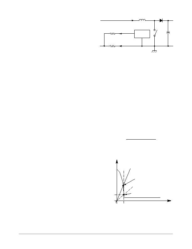
Current Sense
The device senses the inductor current I
L
by the current
senseschemeinFigure32.Thisschemehastheadvantages
of:(1)the inrushcurrentlimitationbythe resistorR
CS
,and
(2) the overcurrent protection and zero current detection
implemented in the same pin.
Figure 32. Current Sensing
CS
NCP1601
Gnd
+
- -
R
CS
R
S
I
L
I
S
I
L
V
S
Inductor current I
L
passes through R
CS
and creates a
negative voltage. This voltage is measured by a current I
S
flowing out of the CS pin (Pin 4). The CS pin has an offset
voltage V
S
. This offset voltage is studied in the setting of
zero inductor current I
L(ZCD)
and the maximum inductor
current I
L(OCP)
(i.e., overcurrent protection threshold). A
typical variation of offset voltage V
S
versus sense current
I
S
is shown in Figure 15. Higher the value of the offset
voltage atlowcurrentregioncreateslowerthe zerocurrent
threshold for better accuracy. Based on Figure 32, (eq.13)
is derived.
(eq.13)
V
S
R
S
I
S
= - -R
CS
I
L
Zero Current Detection (ZCD)
ThedevicerecognizeszeroinductorcurrentwhentheCS
pin (Pin 4) sense current I
S
is lower than I
S(ZCD)
(14 mA
typical). The offset voltage of the CS pin in this condition
is V
S(ZCD)
(7.5 mV typical). It is illustrated in Figure 33.
The inductor current I
L(ZCD)
at the ZCD condition is
derived in (eq.14).
(eq.14)
I
L(ZCD)
=
R
S
I
S(ZCD)
V
S(ZCD)
R
CS
It is obvious that the I
L(ZCD)
is not always zero. In order
to make it reasonably close to zero, the settings of R
S
and
R
CS
are crucial.
Figure 33. CS Pin Characteristic when I
L
= 0
I
S(ZCD)
V
S(ZCD)
R
S
> R
S(ZCD)
R
S
= R
S(ZCD)
V
S
Operating ZCD point
Ideal ZCD point
I
S
相关PDF资料 |
PDF描述 |
|---|---|
| RMC31DRYN-S93 | CONN EDGECARD 62POS DIP .100 SLD |
| RAC03-09SC | CONV AC/DC 3W 9V OUT SINGLE T/H |
| NCP582DSQ28T1G | IC REG LDO 2.8V .15A SC82AB |
| CENB1060A4803F01 | PS EXT 62.4W @ 1.3A DESK E-STAR |
| NCP1653DR2 | IC CTRLR PFC CURRENT MODE 8SOIC |
相关代理商/技术参数 |
参数描述 |
|---|---|
| NCP1601ADR2G | 功能描述:功率因数校正 IC Fixed Frequency DCM/CRM PFC RoHS:否 制造商:Fairchild Semiconductor 开关频率:300 KHz 最大功率耗散: 最大工作温度:+ 125 C 安装风格:SMD/SMT 封装 / 箱体:SOIC-8 封装:Reel |
| NCP1601AGEVB | 功能描述:BOARD EVAL NCP1601A RoHS:是 类别:编程器,开发系统 >> 评估演示板和套件 系列:* 产品培训模块:Obsolescence Mitigation Program 标准包装:1 系列:- 主要目的:电源管理,电池充电器 嵌入式:否 已用 IC / 零件:MAX8903A 主要属性:1 芯锂离子电池 次要属性:状态 LED 已供物品:板 |
| NCP1601AP | 功能描述:功率因数校正 IC Fixed Frequency RoHS:否 制造商:Fairchild Semiconductor 开关频率:300 KHz 最大功率耗散: 最大工作温度:+ 125 C 安装风格:SMD/SMT 封装 / 箱体:SOIC-8 封装:Reel |
| NCP1601APG | 功能描述:功率因数校正 IC Fixed Frequency DCM/CRM PFC RoHS:否 制造商:Fairchild Semiconductor 开关频率:300 KHz 最大功率耗散: 最大工作温度:+ 125 C 安装风格:SMD/SMT 封装 / 箱体:SOIC-8 封装:Reel |
| NCP1601BDR2 | 功能描述:功率因数校正 IC Fixed Frequency RoHS:否 制造商:Fairchild Semiconductor 开关频率:300 KHz 最大功率耗散: 最大工作温度:+ 125 C 安装风格:SMD/SMT 封装 / 箱体:SOIC-8 封装:Reel |
发布紧急采购,3分钟左右您将得到回复。