- 您现在的位置:买卖IC网 > Datasheet目录45 > NCP1601BDR2G (ON Semiconductor)IC PFC CTRL CRM/TRANSITION 8SOIC Datasheet资料下载
参数资料
| 型号: | NCP1601BDR2G |
| 厂商: | ON Semiconductor |
| 文件页数: | 11/19页 |
| 文件大小: | 257K |
| 描述: | IC PFC CTRL CRM/TRANSITION 8SOIC |
| 产品变化通告: | NCP1601BDR2G Discontinuation 11/May/2012 |
| 标准包装: | 1 |
| 模式: | 临界传导(CRM),间歇式(转换) |
| 频率 - 开关: | 58kHz |
| 电流 - 启动: | 17µA |
| 电源电压: | 9.6 V ~ 18 V |
| 工作温度: | -40°C ~ 125°C |
| 安装类型: | 表面贴装 |
| 封装/外壳: | 8-SOIC(0.154",3.90mm 宽) |
| 供应商设备封装: | 8-SOICN |
| 包装: | 剪切带 (CT) |
| 其它名称: | NCP1601BDR2GOSCT |
NCP1601A, NCP1601B
http://onsemi.com
11
be too bulky because it can pollute the power factor by
distorting the rectified sinusoidal input voltage.
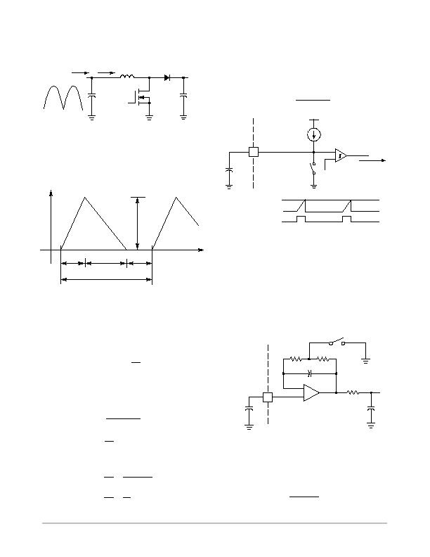
Figure 26. DCM/CRM PFC Boost Converter
V
in
I
in
I
L
L
V
out
C
bulk
C
filter
PFC Methodology
NCP1601 uses a proprietary PFC methodology
particularly designed for both DCM and CRM operation.
The PFC methodology is described in this section.
Figure 27. Inductor Current in DCM
t
1
t
2
t
3
I
pk
T
time
Inductor Current
As shown in Figure 27, the inductor current I
L
of each
switchingcycle startsfromzeroinDCM. CRMis a special
case of DCM when t
3
= 0. When the PFC boost converter
MOSFET ison, the inductorcurrentI
L
increases fromzero
to I
pk
for a time duration t
1
with inductance L and input
voltage V
in
. (eq.1) is formulated.
V
in
= L
I
pk
t
1
(eq.1)
The inputfiltercapacitorC
filter
andthe front- -endedEMI
filter absorb the high- -frequency component of inductor
current. It makes the input current I
in
a low- -frequency
signal.
I
in
=
I
pk
(t
1
+ t
2
)
2 T
(eq.2a)
for DCM
I
in
=
I
pk
2
(eq.2b)
for CRM
From (eq.1) and (eq.2), the input impedance Z
in
is
formulated.
Z
in
=
V
in
I
in
=
2TL
t
1
(
t
1
+ t
2
)
(eq.3a)
for DCM
Z
in
=
V
in
I
in
=
2L
t
1
(eq.3b)
for CRM
Power factor is corrected when the input impedance Z
in
in (eq.3) are constant or slowly varying.
The MOSFET on time t
1
or PFC modulation duty is
generatedbyafeedbacksignalV
ton
andaramp. ThePFC
modulation circuit and timing diagram are shown in
Figure 28. A relationship in (eq.4) is obtained.
t
1
=
C
ramp
V
ton
I
ch
(eq.4)
Figure 28. PFC Modulation Circuit and Timing
Diagram
- -
+
closed when
output low
PFC
Modulation
Turns off
MOSFET
Ramp
3
C
ramp
I
ch
V
ton
V
ton
ramp
output
The charging current I
ch
is constant 100 mA current and
therampcapacitorC
ramp
isconstantforaparticulardesign.
Hence, according to (eq.4) the MOSFET on time t
1
is
proportional to V
ton
.
In order to protect the PFC modulation comparator, the
maximum voltage of V
ton
is limited to internal clamp
V
ton(max)
(3.9 V typical) and the ramp pin (Pin 3) is with a
9 V ESD Zener diode. The 3.9 V maximum limit of this
V
ton
indirectly limits the maximum on time.
Figure 29. V
control
Processing Circuit
+
- -
closed when zero current
2
C
control
V
control
R
1
R
2
R
3
C
1
C
3
V
ton
The V
control
processing circuit generates V
ton
from
control voltage V
control
and time information of zero
inductor current. The circuit in Figure 29 makes (eq.5)
wherethevalueofresistorR
1
ismuchhigherthanthevalue
of resistor R
2
(R
1
>> R
2
).
V
ton
=
T V
control
t
1
+ t
2
(eq.5a)
for DCM
相关PDF资料 |
PDF描述 |
|---|---|
| NCP1603D100R2G | IC CTLR PFC/PWM COMBO 16-SOIC |
| NCP1605DR2G | IC PFC CONTROLLER CCM/DCM 16SOIC |
| NCP1606BDR2G | IC POWER FACTOR CONTROLLER 8SOIC |
| NCP1607BDR2G | IC PFC CONTROLLER CRM 8SOIC |
| NCP1611BDR2G | IC PFC CTLR HE ENHANCED 8-SOIC |
相关代理商/技术参数 |
参数描述 |
|---|---|
| NCP1601BP | 功能描述:功率因数校正 IC Fixed Frequency RoHS:否 制造商:Fairchild Semiconductor 开关频率:300 KHz 最大功率耗散: 最大工作温度:+ 125 C 安装风格:SMD/SMT 封装 / 箱体:SOIC-8 封装:Reel |
| NCP1601BPG | 功能描述:功率因数校正 IC Fixed Frequency DCM/CRM PFC RoHS:否 制造商:Fairchild Semiconductor 开关频率:300 KHz 最大功率耗散: 最大工作温度:+ 125 C 安装风格:SMD/SMT 封装 / 箱体:SOIC-8 封装:Reel |
| NCP1603D100R2 | 功能描述:功率因数校正 IC High Voltage Startup RoHS:否 制造商:Fairchild Semiconductor 开关频率:300 KHz 最大功率耗散: 最大工作温度:+ 125 C 安装风格:SMD/SMT 封装 / 箱体:SOIC-8 封装:Reel |
| NCP1603D100R2G | 功能描述:功率因数校正 IC ANA PFC/PWM COMBO CONTROL RoHS:否 制造商:Fairchild Semiconductor 开关频率:300 KHz 最大功率耗散: 最大工作温度:+ 125 C 安装风格:SMD/SMT 封装 / 箱体:SOIC-8 封装:Reel |
| NCP1605ADR2G | 功能描述:功率因数校正 IC ENHANCED PFC CNTRLER RoHS:否 制造商:Fairchild Semiconductor 开关频率:300 KHz 最大功率耗散: 最大工作温度:+ 125 C 安装风格:SMD/SMT 封装 / 箱体:SOIC-8 封装:Reel |
发布紧急采购,3分钟左右您将得到回复。