- 您现在的位置:买卖IC网 > Datasheet目录45 > NCP1601BDR2G (ON Semiconductor)IC PFC CTRL CRM/TRANSITION 8SOIC Datasheet资料下载
参数资料
| 型号: | NCP1601BDR2G |
| 厂商: | ON Semiconductor |
| 文件页数: | 12/19页 |
| 文件大小: | 257K |
| 描述: | IC PFC CTRL CRM/TRANSITION 8SOIC |
| 产品变化通告: | NCP1601BDR2G Discontinuation 11/May/2012 |
| 标准包装: | 1 |
| 模式: | 临界传导(CRM),间歇式(转换) |
| 频率 - 开关: | 58kHz |
| 电流 - 启动: | 17µA |
| 电源电压: | 9.6 V ~ 18 V |
| 工作温度: | -40°C ~ 125°C |
| 安装类型: | 表面贴装 |
| 封装/外壳: | 8-SOIC(0.154",3.90mm 宽) |
| 供应商设备封装: | 8-SOICN |
| 包装: | 剪切带 (CT) |
| 其它名称: | NCP1601BDR2GOSCT |
NCP1601A, NCP1601B
http://onsemi.com
12
V
ton
= V
control
(eq.5b)
for CRM
It is noted that V
ton
is always greater than or equal to
V
control
(i.e., V
ton
?V
control
).
Insummary,theinputimpedanceZ
in
in(eq.6)isobtained
from (eq.1)- -(eq.5)
Z
in
=
V
in
I
in
=
2 L I
ch
C
ramp
V
control
(eq.6)
Control voltage V
control
comes from the PFC output
voltage V
out
which is a slowly varying signal. The
bandwidth of V
control
can be additionally limited by
inserting an external capacitor C
control
to the V
control
pin
(Pin 2) in Figure 28. The internal 300 k?resistor and the
capacitor C
control
create a low- -pass filter which has a
bandwidthf
control
in(eq.7).Itisgenerallyrecommendedto
limit the bandwidth below 20 Hz to achieve power factor
correction. Typical value of C
control
is 0.1 mF.
C
control
>
1
2?00k?f
control
(eq.7)
If the bandwidth of V
control
is much less than the 50 or
60 Hz line frequency, the input impedance Z
in
is slowly
varying or roughly constant. Then, the power factor
correction is achieved in DCM and CRM.
Figure 30. V
control
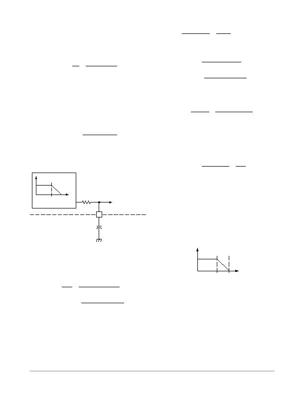
Low- -Pass Filtering
300k
Regulation Block
2
C
control
V
control
V
reg
I
ref
I
ref
96%
I
FB
V
control
Processing
Circuit
Maximum Power
Input and output power (P
in
and P
out
) are derived in
(eq.8)whenthecircuitefficiency穒sobtainedorassumed.
The variable V
ac
stands for the RMS input voltage.
(eq.8a)
P
in
=
V
ac
2
Z
in
=
V
ac
2
C
ramp
V
control
2LI
ch
(eq.8b)
P
out
= ?P
in
=
稸
ac
2
C
ramp
V
control
2LI
ch
From(eq.8), controlvoltage V
control
controlstheamount
of output power, input power, or input impedance. The
maximum value of the control voltage V
control
is 1.05 V
(i.e., V
control(max)
=1.05V). Aparameter calledmaximum
powerresistorR
power
(10.5 k﹖ypical) isdefined in(eq.9)
and restricted to have a maximum ?0% variation
(i.e.,9.5kR
power
?1.5k?fordefiningthemaximum
power in an application.
R
power
=
V
control(max)
I
ch
=
1.05 V
100 mA
= 10.5 k?/DIV>
(eq.9)
It means that the maximum input and output power
(P
in(max)
and P
out(max)
) are limited to ?0% variation.
(eq.10a)
P
in(max)
=
V
ac
2
C
ramp
R
power
2 L
(eq.10b)
P
out(max)
=
稸
ac
2
C
ramp
R
power
2 L
The maximum input current I
ac(max)
to deliver the
maximum input power P
in(max)
is also derived in (eq.11).
The suffix ac stands for RMS value.
(eq.11)
I
ac(max)
=
P
in(max)
V
ac
=
V
acC
ramp
R
power
2 L
Output Feedback
The output voltage V
out
of the PFC circuit is sensed as a
feedback current I
FB
flowing into the FB pin (Pin 1) of the
device. The FB pin voltage V
FB1
is typically less than 5 V
referring to Figure 11. It is much lower than V
out
which is
typically 400 V. Therefore, V
FB1
is generally neglected.
(eq.12)
I
FB
=
V
out
V
FB1
R
FB
H
V
out
R
FB
where R
FB
is the feedback resistor connected between the
FB pin (Pin 1) and the output voltage referringto Figure 2.
Then, the feedback current I
FB
represents the output
voltage V
out
and will be used in the output voltage
regulation, Undervoltage Protection (UVP), and
Overvoltage Protection (OVP).
Output Voltage Regulation
Feedback current I
FB
, which presents output voltage
V
out
, is regulated with a reference current (I
ref
= 203 mA
typical) as shown in Figure 31.
Figure 31. Regulation Block
V
reg
I
ref
I
ref
96%
I
FB
1.05 V
When I
FB
is lower than 96% of I
ref
, the V
reg
which isthe
output of the regulation block is as high as V
control(max)
(1.05Vtypical)thatgivesthe maximumvalue onV
ton
. As
a result, it gives the maximum MOSFET on time and V
out
increases. When I
FB
is higher than I
ref
, the V
reg
becomes 0
V that gives no MOSFET on time and V
out
decreases. As
a result, the output voltage V
out
is regulated around the
range between96% and100% ofthe nominalvalue ofR
FB
?I
ref
.
Based on (eq.8) for a particular power level, the V
control
is inversely proportional to V
ac
2
. Hence, in high V
ac
condition V
control
is lower. It means that I
FB
or output
相关PDF资料 |
PDF描述 |
|---|---|
| NCP1603D100R2G | IC CTLR PFC/PWM COMBO 16-SOIC |
| NCP1605DR2G | IC PFC CONTROLLER CCM/DCM 16SOIC |
| NCP1606BDR2G | IC POWER FACTOR CONTROLLER 8SOIC |
| NCP1607BDR2G | IC PFC CONTROLLER CRM 8SOIC |
| NCP1611BDR2G | IC PFC CTLR HE ENHANCED 8-SOIC |
相关代理商/技术参数 |
参数描述 |
|---|---|
| NCP1601BP | 功能描述:功率因数校正 IC Fixed Frequency RoHS:否 制造商:Fairchild Semiconductor 开关频率:300 KHz 最大功率耗散: 最大工作温度:+ 125 C 安装风格:SMD/SMT 封装 / 箱体:SOIC-8 封装:Reel |
| NCP1601BPG | 功能描述:功率因数校正 IC Fixed Frequency DCM/CRM PFC RoHS:否 制造商:Fairchild Semiconductor 开关频率:300 KHz 最大功率耗散: 最大工作温度:+ 125 C 安装风格:SMD/SMT 封装 / 箱体:SOIC-8 封装:Reel |
| NCP1603D100R2 | 功能描述:功率因数校正 IC High Voltage Startup RoHS:否 制造商:Fairchild Semiconductor 开关频率:300 KHz 最大功率耗散: 最大工作温度:+ 125 C 安装风格:SMD/SMT 封装 / 箱体:SOIC-8 封装:Reel |
| NCP1603D100R2G | 功能描述:功率因数校正 IC ANA PFC/PWM COMBO CONTROL RoHS:否 制造商:Fairchild Semiconductor 开关频率:300 KHz 最大功率耗散: 最大工作温度:+ 125 C 安装风格:SMD/SMT 封装 / 箱体:SOIC-8 封装:Reel |
| NCP1605ADR2G | 功能描述:功率因数校正 IC ENHANCED PFC CNTRLER RoHS:否 制造商:Fairchild Semiconductor 开关频率:300 KHz 最大功率耗散: 最大工作温度:+ 125 C 安装风格:SMD/SMT 封装 / 箱体:SOIC-8 封装:Reel |
发布紧急采购,3分钟左右您将得到回复。