- 您现在的位置:买卖IC网 > Datasheet目录45 > NCP1603D100R2G (ON Semiconductor)IC CTLR PFC/PWM COMBO 16-SOIC Datasheet资料下载
参数资料
| 型号: | NCP1603D100R2G |
| 厂商: | ON Semiconductor |
| 文件页数: | 18/30页 |
| 文件大小: | 302K |
| 描述: | IC CTLR PFC/PWM COMBO 16-SOIC |
| 产品变化通告: | Product Discontinuation 21/Jun/2007 |
| 标准包装: | 2,500 |
| 模式: | 临界传导(CRM),间歇导电(DCM) |
| 频率 - 开关: | 58kHz |
| 电流 - 启动: | 17µA |
| 电源电压: | 9 V ~ 18 V |
| 工作温度: | -40°C ~ 125°C |
| 安装类型: | 表面贴装 |
| 封装/外壳: | 16-SOIC(0.154",3.90mm 宽) |
| 供应商设备封装: | 16-SOIC |
| 包装: | 带卷 (TR) |
第1页第2页第3页第4页第5页第6页第7页第8页第9页第10页第11页第12页第13页第14页第15页第16页第17页当前第18页第19页第20页第21页第22页第23页第24页第25页第26页第27页第28页第29页第30页
NCP1603
http://onsemi.com
18
The UVLO start thresholds of V
CC1
is V
CC1(on)
(10.5 V
typical) and the maximum allowable limit is 18 V. On the
other hand, the V
aux
is enabled when V
CC2
is over V
CC2(off)
(7.7 V typical). Hence, there are two possible operating
regions in Figure 49. In the nonusable region the V
aux
is
not high enough to turn on the PFC section. Therefore, the
flyback transformer auxiliary winding must be between
V
CC1(on)
(10.5 V typical) and 18 V.
Regulation in the PWM Section
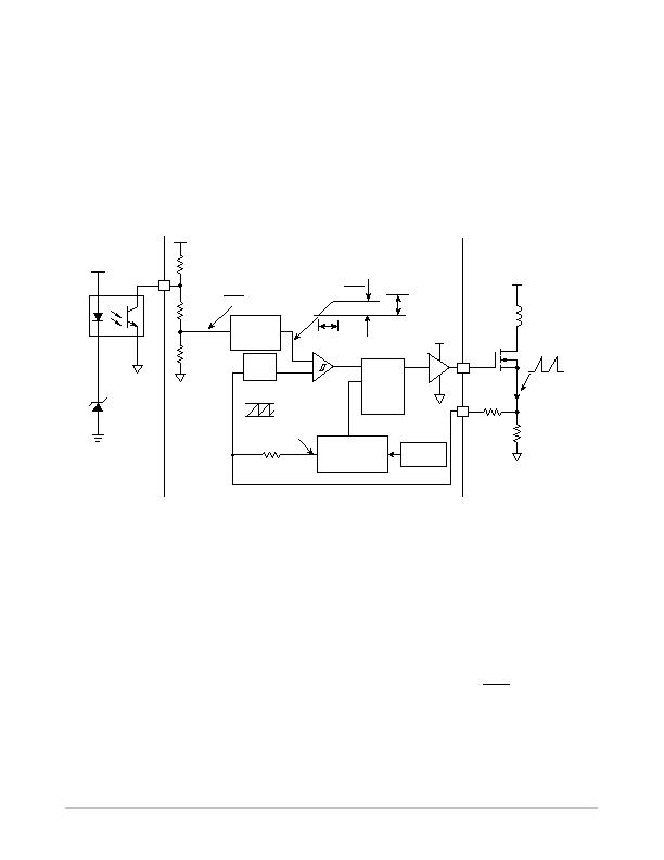
The PWM section (or the second stage) of the NCP1603
is NCP1230 that is a currentmode fixedfrequency PWM
flyback controller with internal compensation ramp. The
simplified block diagram of the duty cycle regulation
section is in Figure 50. A 100 kHz clock oscillator is
modulated by adding a frequency jittering feature. This
modulated 100 kHz clock signal turns the Out2 (pin 13)
high in each switching cycle. The Out2 goes low when the
currentloop feedback signal intersects with the output
voltageloop feedback signal. A duty cycle is therefore
generated. The maximum duty ratio is limited to D
max
(80% typical).
V
out
2
Opto
Coupler
FB2
Vdd
20 k
55 k
25 k
V
FB2
V
FB2
3
SoftStart
Processing
Circuit
-
+
200 ns
LEB
SoftStart Period 2.5 ms
V
FB2
3
1 V Max
PWM
R
S
Q
Max Duty
= 80%
V
CC2
13
3
Out2
V
bulk
Flyback
Drain
Current
I
D
CS2
R
S2
R
CS2
6.4% Frequency
Jittering
Modulation
100 kHz
Oscillator
2.3 V
0 V
100 kHz
Jittering Ramp
18 k
Figure 50. Block Diagram of Duty Cycle Regulation in the PWM Section
The currentloop feedback circuit consists of a typical
200 ns Leading Edge Blanking (LEB) that is to prevent a
premature reset of the output due to noise, a pair of sense
resistors R
CS2
and R
S2
that sense the flyback drain current
I
D
, and a 0to2.3 V jittering ramp that adds a ramp
compensation for a stability improvement to the
currentmode control possibly in continuous mode
operation.
The V
FB2
is approximately divided by 3 by an internal
pair of resistors (55 kW and 25 kW). The softstart
processing circuit reduces the initial voltageloop
feedback signal (V
FB2
/ 3) for 2.5 ms. After this 2.5 ms, the
softstart disappears. As a result, the startup envelope of
the peak drain current (or duty ratio) ramps up gradually for
2.5 ms. It is noted that the 2.5 ms is counted when the PWM
die circuit is reset that is when V
CC2
reaches V
CC2(on)
(12.6 V typical). This softstart feature offers a reduced
transient voltage and current stress on the power circuit
during the startup.
Excessive output voltage causes more the optocoupler
current. It pulls down the V
FB2
through FB2 pin (Pin 2) and
generates a lower duty ratio. The output voltage reduces.
Insufficient output voltage reduces the optocoupler
current. If the current is too small, the V
FB2
is eventually
pulled high than 3.0 V (3.8 V typical). The (V
FB2
/3) signal
is then clamped to an internal 1.0 V limit. If the ramp is
ignored (i.e., R
S2
= 0), the maximum possible drain current
is derived as:
I
D(max)
+
1 V
R
CS2
(eq. 2)
It is noted that resistor R
S2
will affect the percentage of
the ramp getting compared for the modulation. Hence, a
large value of the R
S2
increase the ramp and will reduce the
possible maximum duty ratio.
相关PDF资料 |
PDF描述 |
|---|---|
| NCP1605DR2G | IC PFC CONTROLLER CCM/DCM 16SOIC |
| NCP1606BDR2G | IC POWER FACTOR CONTROLLER 8SOIC |
| NCP1607BDR2G | IC PFC CONTROLLER CRM 8SOIC |
| NCP1611BDR2G | IC PFC CTLR HE ENHANCED 8-SOIC |
| NCP1651DR2G | IC PFC CONTROLLER CCM/DCM 16SOIC |
相关代理商/技术参数 |
参数描述 |
|---|---|
| NCP1605ADR2G | 功能描述:功率因数校正 IC ENHANCED PFC CNTRLER RoHS:否 制造商:Fairchild Semiconductor 开关频率:300 KHz 最大功率耗散: 最大工作温度:+ 125 C 安装风格:SMD/SMT 封装 / 箱体:SOIC-8 封装:Reel |
| NCP1605BDR2G | 功能描述:功率因数校正 IC High Volt Stby Mode Power Fact Corr Cont RoHS:否 制造商:Fairchild Semiconductor 开关频率:300 KHz 最大功率耗散: 最大工作温度:+ 125 C 安装风格:SMD/SMT 封装 / 箱体:SOIC-8 封装:Reel |
| NCP1605DR2G | 功能描述:功率因数校正 IC Enhanced PFC HV and Eff Standby RoHS:否 制造商:Fairchild Semiconductor 开关频率:300 KHz 最大功率耗散: 最大工作温度:+ 125 C 安装风格:SMD/SMT 封装 / 箱体:SOIC-8 封装:Reel |
| NCP1605FORWGEVB | 功能描述:电源管理IC开发工具 NCP1605 152 W FORWARD EVB RoHS:否 制造商:Maxim Integrated 产品:Evaluation Kits 类型:Battery Management 工具用于评估:MAX17710GB 输入电压: 输出电压:1.8 V |
| NCP1605LCDTVGEVB | 功能描述:BOARD EVAL NCP1605/1396 RoHS:是 类别:编程器,开发系统 >> 评估演示板和套件 系列:* 产品培训模块:Obsolescence Mitigation Program 标准包装:1 系列:- 主要目的:电源管理,电池充电器 嵌入式:否 已用 IC / 零件:MAX8903A 主要属性:1 芯锂离子电池 次要属性:状态 LED 已供物品:板 |
发布紧急采购,3分钟左右您将得到回复。