参数资料
| 型号: | NCP1608BOOSTGEVB |
| 厂商: | ON Semiconductor |
| 文件页数: | 15/24页 |
| 文件大小: | 0K |
| 描述: | BOARD EVAL NCP1608 100W BOOST |
| 设计资源: | NCP1608BOOSTGEVB Schematic NCP1608BOOSTGEVB Gerber Files NCP1608BOOSTGEVB Bill of Materials |
| 标准包装: | 1 |
| 主要目的: | 电源管理,功率因数校正 |
| 嵌入式: | 否 |
| 已用 IC / 零件: | NCP1608 |
| 主要属性: | 100 W,85 ~ 265 VAC 输入,400 VDC 稳压输出 |
| 已供物品: | 板 |
| 其它名称: | NCP1608BOOSTGEVB-ND NCP1608BOOSTGEVBOS |
�� �
�
�NCP1608�
�V� in�
�N� B�
�N� ZCD�
�+�
�?�
�S�
�Q�
�Reset�
�Demag�
�R� sense�
�V� ZCD(ARM)�
�+�
�?�
�DRIVE�
�Dominant�
�Latch�
�R� Q�
�V� ZCD(TRIG)�
�ZCD�
�R� ZCD�
�ZCD� Clamp�
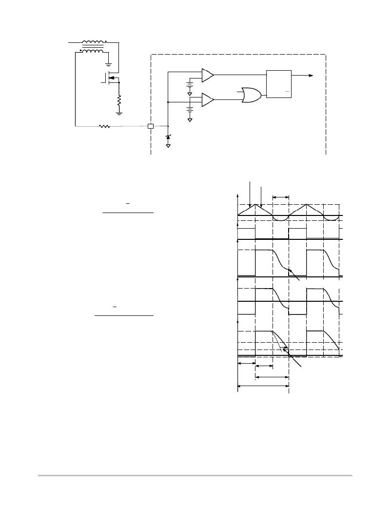
�Figure� 33.� Implementation� of� the� ZCD� Block�
�I� L�
�This� sequence� achieves� CrM� operation.� The� maximum�
�V� ZCD(ARM)� sets� the� maximum� turns� ratio� and� is� calculated�
�using� Equation� 11:�
�MOSFET� Conduction�
�Diode� Conduction�
�t� z�
�N� B� :� N� ZCD� v�
�V� ZCD(ARM)�
�V� out� *� 2� @� Vac� HL�
�(eq.� 11)�
�Where� Vac� HL� is� the� maximum� rms� input� voltage� and�
�V� ZCD(ARM)� =� 1.55� V� (maximum� value).�
�The� NCP1608� prevents� excessive� voltages� on� the� ZCD�
�pin� by� clamping� V� ZCD� .� When� the� ZCD� winding� is� negative,�
�the� ZCD� pin� is� internally� clamped� to� V� CL(NEG)� .� Similarly,�
�when� the� ZCD� winding� is� positive,� the� ZCD� pin� is�
�internally� clamped� to� V� CL(POS)� .� A� resistor� (R� ZCD� in�
�Figure� 33)� is� necessary� to� limit� the� current� into� the� ZCD�
�pin.� The� maximum� ZCD� pin� current� (I� ZCD(MAX)� )� is� limited�
�to� less� than� 10� mA.� R� ZCD� is� calculated� using� Equation� 12:�
�I� L(peak)�
�I� L(NEG)�
�DRV�
�V� drain�
�V� out�
�V� ZCD(WIND)�
�V� ZCD(WIND),off�
�0A�
�0V�
�0V�
�Minimum Voltage Turn on�
�0V�
�R� ZCD� w�
�2� @� Vac� HL�
�I� ZCD(MAX)� @� (N� B� :� N� ZCD� )�
�(eq.� 12)�
�The� value� of� R� ZCD� and� the� parasitic� capacitance� of� the�
�ZCD� pin� determine� when� the� ZCD� winding� signal� is�
�detected� and� the� drive� turn� on� begins.� A� large� R� ZCD� value�
�creates� a� long� delay� before� detecting� the� ZCD� event.� In� this�
�case,� the� controller� operates� in� DCM� and� the� power� factor�
�is� reduced.� If� the� R� ZCD� value� is� too� small,� the� drive� turns�
�on� when� the� drain� voltage� is� high� and� efficiency� is� reduced.�
�V� ZCD(WIND),on�
�V� ZCD�
�V� CL(POS)�
�V� ZCD(ARM)�
�V� ZCD(TRIG)�
�V� CL(NEG)�
�t� on�
�t� diode�
�t� off�
�R� ZCD� Delay�
�0V�
�A� popular� strategy� for� selecting� R� ZCD� is� to� use� the� R� ZCD�
�value� that� achieves� minimum� drain� voltage� turn� on.� This�
�value� is� found� experimentally.� Figure� 34� shows� the� realistic�
�waveforms� for� CrM� operation� due� to� R� ZCD� and� the� ZCD� pin�
�capacitance.�
�T� SW�
�Figure� 34.� Realistic� CrM� Waveforms� Using� a� ZCD�
�Winding� with� R� ZCD� and� the� ZCD� Pin� Capacitance�
�http://onsemi.com�
�15�
�相关PDF资料 |
PDF描述 |
|---|---|
| NCP1631PFCGEVB | BOARD DEMO NCP1631 INTERLEAV PFC |
| NCP1650EVB | BOARD EVAL NCP1650 PFC CTLR |
| NCP1652L48VGEVB | BOARD EVAL 100W 48V NCP1652 PFC |
| NCP1653EVB | BOARD EVAL FOR NCP1653 |
| NCP2993FCT2GEVB | BOARD EVAL NCP2993 AUDIO PWR AMP |
相关代理商/技术参数 |
参数描述 |
|---|---|
| NCP1611ADR2G | 功能描述:功率因数校正 IC NCP1611A ENHANCED PFC RoHS:否 制造商:Fairchild Semiconductor 开关频率:300 KHz 最大功率耗散: 最大工作温度:+ 125 C 安装风格:SMD/SMT 封装 / 箱体:SOIC-8 封装:Reel |
| NCP1611BDR2G | 功能描述:功率因数校正 IC NCP1611A ENHANCED PFC RoHS:否 制造商:Fairchild Semiconductor 开关频率:300 KHz 最大功率耗散: 最大工作温度:+ 125 C 安装风格:SMD/SMT 封装 / 箱体:SOIC-8 封装:Reel |
| NCP1611GEVB | 制造商:ON Semiconductor 功能描述:PG - ACDC CONVERSION - Bulk 制造商:ON Semiconductor 功能描述:EVAL BOARD, NCP1611, POWER FACTOR CORRECTION; Silicon Manufacturer:On Semiconductor; Silicon Core Number:NCP1611; Kit Application Type:Power Management; Application Sub Type:Power Factor Correction (PFC) ;RoHS Compliant: Yes |
| NCP1612ADR2G | 功能描述:功率因数校正 IC RoHS:否 制造商:Fairchild Semiconductor 开关频率:300 KHz 最大功率耗散: 最大工作温度:+ 125 C 安装风格:SMD/SMT 封装 / 箱体:SOIC-8 封装:Reel |
| NCP1612BDR2G | 制造商:ON Semiconductor 功能描述:ENHANCED HIGH-EFFICIENCY - Tape and Reel |
发布紧急采购,3分钟左右您将得到回复。