- 您现在的位置:买卖IC网 > PDF目录22197 > NCP1654BP65G (ON Semiconductor)IC PFC CCM STEP UP 8-PDIP PDF资料下载
参数资料
| 型号: | NCP1654BP65G |
| 厂商: | ON Semiconductor |
| 文件页数: | 16/23页 |
| 文件大小: | 228K |
| 描述: | IC PFC CCM STEP UP 8-PDIP |
| 标准包装: | 50 |
| 模式: | 连续导电(CCM) |
| 频率 - 开关: | 58kHz ~ 72kHz |
| 电流 - 启动: | 75µA |
| 电源电压: | 9 V ~ 20 V |
| 工作温度: | -40°C ~ 125°C |
| 安装类型: | 通孔 |
| 封装/外壳: | 8-DIP(0.300",7.62mm) |
| 供应商设备封装: | 8-PDIP |
| 包装: | 管件 |
| 其它名称: | NCP1654BP65GOS |
NCP1654
http://onsemi.com
16
Input and output power (P
in
and P
out
) are derived in (Equation 15) when the circuit efficiency ?is obtained or assumed.
The variable V
ac
stands for the rms input voltage.
P
in
+
V
ac
2
Z
in
+
2pR
CS
@ (V
control
* V
CONTROL(min)
) @ V
REF
@ V
ac
2
R
M
R
SENSE
V
out
K
BO
(eq. 15)
T
(V
control
* V
CONTROL(min)
)V
ac
V
out
P
out
+ h P
in
+ h
2pR
CS
@ (V
control
* V
CONTROL(min)
) @ V
REF
@ V
ac
2
R
M
R
SENSE
V
out
K
BO
(eq. 16)
T
(V
control
* V
CONTROL(min)
)V
ac
V
out
Follower Boost
The
Follower Boost
is an operation mode where the
preconverter output voltage stabilizes at a level that varies
linearly versus the ac line amplitude. This technique aims
at reducing the gap between the output and input voltages
to optimize the boost efficiency and minimize the cost of
the PFC stage (refer to MC33260 data sheet for more
details at http://www.onsemi.com
).
The NCP1654 operates in follower boost mode when
V
control
is constant, i.e. V
control
raises to its maximum value
V
CONTROL(max)
. Reformulate (Equation 16) to become
(Equation 17) and (Equation 18) by replace V
control
by
V
CONTROL(max)
. If V
control
is constant based on
(Equation 15), for a constant load or power demand the
output voltage V
out
of the converter is proportional to the
rms input voltage V
ac
. It means the output voltage V
out
becomes lower when the rms input voltage V
ac
becomes
lower. On the other hand, the output voltage V
out
becomes
lower when the load or power demand becomes higher.
P
out
+ h
2pR
CS
@ (V
CONTROL(max)
* V
CONTROL(min)
) @ V
REF
@ V
ac
2
R
M
R
SENSE
V
out
K
BO
(eq. 17)
+ h
2pR
CS
@ DV
CONTROL
@ V
REF
@ V
ac
2
R
M
R
SENSE
V
out
K
BO
V
out
+ h
2pR
CS
@ DV
CONTROL
@ V
REF
2
R
M
R
SENSE
K
BO
@
V
ac
P
out
(eq. 18)
where
V
CONTROL(max)
is the maximum control voltage.
DV
CONTROL
is the gap between V
CONTROL(max)
and
V
CONTROL(min)
.
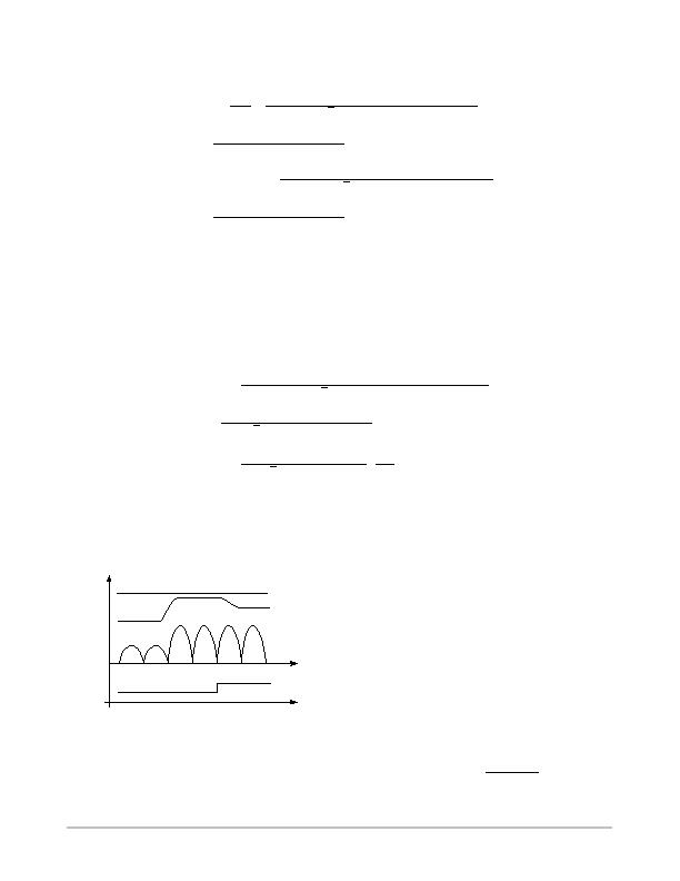
It is illustrated in Figure 39.
Figure 39. Follower Boost Characteristics
V
out
(Traditional Boost)
V
out
(Follower Boost)
V
in
P
out
Time
Time
Follower Boost Benefits
The follower boost circuit offers and opportunity to
reduce the output voltage V
out
whenever the rms input
voltage V
ac
is lower or the power demand P
out
is higher.
Because of the stepup characteristics of boost converter,
the output voltage V
out
will always be higher than the input
voltage V
in
even though V
out
is reduced in follower boost
operation. As a result, the on time t
1
is reduced. Reduction
of on time makes the loss of the inductor and power
MOSFET smaller. Hence, it allows cheaper cost in the
inductor and power MOSFET or allows the circuit
components to operate at a lower stress condition in most
of the time.
Reference Section
The internal reference voltage (V
REF
) is trimmed to be
?% accurate over the temperature range (the typical value
is 2.5 V). V
REF
is the reference used for the regulation.
V
REF
also serves to build the thresholds of the fast transient
response, Overvoltage (OVP), brown out (BO), and
Undervoltage protections (UVP).
Output Feedback
The output voltage V
out
of the PFC circuits is sensed at
V
fb
pin via the resistor divider (R
fbL
and R
fbU
) as shown in
Figure 38. V
out
is regulated as described in (Equation 19).
V
out
+ V
REF
R
fbU
) R
fbL
R
fbL
(eq. 19)
相关PDF资料 |
PDF描述 |
|---|---|
| RAC05-05SA-E | CONV AC/DC 90-264VAC 5V 1A |
| VE-J10-IZ | CONVERTER MOD DC/DC 5V 25W |
| FAN6961DY | IC PFC CONTROLLER DCM 8DIP |
| RAC10-3.3SA-E | CONV AC/DC 90-264VAC 3.3V 3A |
| RBM08DRYS | CONN EDGECARD 16POS DIP .156 SLD |
相关代理商/技术参数 |
参数描述 |
|---|---|
| NCP1654PFCGEVB | 功能描述:电源管理IC开发工具 NCP1654 PWR FACT CONT EVB RoHS:否 制造商:Maxim Integrated 产品:Evaluation Kits 类型:Battery Management 工具用于评估:MAX17710GB 输入电压: 输出电压:1.8 V |
| NCP1729-SKT | 制造商:P&S 功能描述:Sample Kit, including Two NCP1729SN35T1 and A Development Source CD-ROM 制造商:P&S 功能描述:Sample Kit,including Two NCP1729SN35T1 and A Development Source CD-ROM |
| NCP1729SN35T1 | 功能描述:电荷泵 Switched Cap Voltage RoHS:否 制造商:Maxim Integrated 功能:Inverting, Step Up 输出电压:- 1.5 V to - 5.5 V, 3 V to 11 V 输出电流:100 mA 电源电流:1 mA 最大工作温度:+ 70 C 封装 / 箱体:SOIC-8 Narrow 封装:Tube |
| NCP1729SN35T1G | 功能描述:电荷泵 Switched Cap Voltage Inverter w/Shutdown RoHS:否 制造商:Maxim Integrated 功能:Inverting, Step Up 输出电压:- 1.5 V to - 5.5 V, 3 V to 11 V 输出电流:100 mA 电源电流:1 mA 最大工作温度:+ 70 C 封装 / 箱体:SOIC-8 Narrow 封装:Tube |
| NCP1729SN35T1G | 制造商:ON Semiconductor 功能描述:Power Supply IC |
发布紧急采购,3分钟左右您将得到回复。