- 您现在的位置:买卖IC网 > PDF目录13711 > NCP3163BMNR2G (ON Semiconductor)IC REG BUCK BOOST INV ADJ DFN18 PDF资料下载
参数资料
| 型号: | NCP3163BMNR2G |
| 厂商: | ON Semiconductor |
| 文件页数: | 3/20页 |
| 文件大小: | 0K |
| 描述: | IC REG BUCK BOOST INV ADJ DFN18 |
| 标准包装: | 1 |
| 类型: | 降压(降压),升压(升压),反相 |
| 输出类型: | 可调式 |
| 输出数: | 1 |
| 输出电压: | 可调至 40V |
| 输入电压: | 2.5 V ~ 40 V |
| PWM 型: | 混合物 |
| 频率 - 开关: | 50kHz ~ 300kHz |
| 电流 - 输出: | 3.4A |
| 同步整流器: | 无 |
| 工作温度: | -40°C ~ 85°C |
| 安装类型: | 表面贴装 |
| 封装/外壳: | 18-VFDFN 裸露焊盘 |
| 包装: | 剪切带 (CT) |
| 供应商设备封装: | 18-DFN(5x6) |
| 其它名称: | NCP3163BMNR2GOSCT |
�� �
�
�NCP3163,� NCV3163�
�MAXIMUM� RATINGS� (Note� 1)�
�Rating�
�Power� Supply� Voltage�
�Switch� Collector� Voltage� Range�
�Switch� Emitter� Voltage� Range�
�Switch� Collector� to� Emitter� Voltage�
�Switch� Current�
�Driver� Collector� Voltage� (Pin� 8)�
�Driver� Collector� Current� (Pin� 8)�
�Bootstrap� Input� Current� Range�
�Current� Sense� Input� Voltage� Range�
�Feedback� and� Timing� Capacitor� Input� Voltage� Range�
�Low� Voltage� Indicator� Output� Voltage� Range�
�Low� Voltage� Indicator� Output� Sink� Current�
�Symbol�
�V� CC�
�V� CSW�
�V� ESW�
�V� CESW�
�I� SW�
�V� CC�
�I� CC�
�I� BST�
�V� IPKSNS�
�V� in�
�V� CLVI�
�I� CLVI�
�Value�
�0� to� +40�
�?� 1.0� to� +40�
�?� 2.0� to� +40�
�+40�
�3.4�
�?� 1.0� to� +40�
�150�
�?� 100� to� +100�
�(V� CC� ?� 7.0)� to� (V� CC� +� 1.0)�
�?� 1.0� to� +7.0�
�?� 1.0� to� +40�
�10�
�Unit�
�V�
�V�
�V�
�V�
�A�
�V�
�mA�
�mA�
�V�
�V�
�V�
�mA�
�Power� Dissipation� and� Thermal� Characteristics�
�Thermal� Characteristics�
�Thermal� Resistance,� Junction� ?� to� ?� Case�
�Thermal� Resistance,� Junction� ?� to� ?� Air�
�Storage� Temperature� Range�
�Maximum� Junction� Temperature�
�Operating� Ambient� Temperature� (Note� 3)�
�NCP3163�
�NCP3163B�
�NCV3163�
�R� q� JC�
�R� q� JA�
�T� stg�
�T� Jmax�
�T� A�
�15�
�56�
�?� 65� to� +150�
�+150�
�0� to� +70�
�?� 40� to� +85�
�?� 40� to� +125�
�°� C/W�
�°� C�
�°� C�
�°� C�
�Stresses� exceeding� Maximum� Ratings� may� damage� the� device.� Maximum� Ratings� are� stress� ratings� only.� Functional� operation� above� the�
�Recommended� Operating� Conditions� is� not� implied.� Extended� exposure� to� stresses� above� the� Recommended� Operating� Conditions� may� affect�
�device� reliability.�
�1.� This� device� series� contains� ESD� protection� and� exceeds� the� following� tests:�
�Human� Body� Model� 2000� V� per� MIL� ?� STD� ?� 883,� Method� 3015.�
�Machine� Model� Method� 200� V.�
�Charged� Device� Model� 750� V� for� corner� pins� and� 500� V� for� others� (according� to� AEC� ?� Q100).�
�2.� This� device� contains� latch� ?� up� protection� and� exceeds� 100� mA� per� JEDEC� Standard� JESD78.�
�3.� Maximum� package� power� dissipation� limits� must� be� observed.� Maximum� Junction� Temperature� must� not� be� exceeded.�
�4.� The� pins� which� are� not� defined� may� not� be� loaded� by� external� signals.�
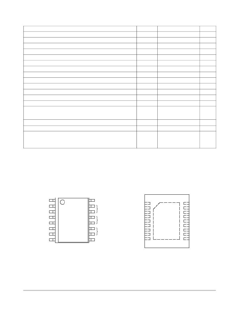
�PIN� CONNECTIONS�
�LVI� Output�
�Voltage� Feedback� 2�
�Voltage� Feedback� 1�
�GND�
�N/C�
�Timing� Capacitor�
�V� CC�
�I� pk� Sense�
�1�
�2�
�3�
�4�
�5�
�6�
�7�
�8�
�16�
�15�
�14�
�13�
�12�
�11�
�10�
�9�
�Bootstrap� Input�
�Switch�
�Emitter�
�N/C�
�Switch� Collector�
�Driver� Collector�
�Timing� Capacitor�
�N/C�
�V� CC�
�I� pk� Sense�
�Driver� Collector�
�Switch� Collector�
�Switch� Collector�
�Switch� Collector�
�Switch� Collector�
�1�
�2�
�3�
�4�
�5�
�6�
�7�
�8�
�9�
�GND�
�EP� Flag�
�18�
�17�
�16�
�15�
�14�
�13�
�12�
�11�
�10�
�GND�
�Voltage� Feedback� 1�
�Voltage� Feedback� 2�
�LVI� Output�
�Bootstrap� Input�
�Switch� Emitter�
�Switch� Emitter�
�Switch� Emitter�
�Switch� Emitter�
�(Top� View)�
�Note:� Pin� 18� must� be� tied� to� EP� Flag� on� PCB�
�http://onsemi.com�
�3�
�相关PDF资料 |
PDF描述 |
|---|---|
| MAX6726AKAVDD6+T | IC SUPERVISOR MPU SOT23-8 |
| VI-J4Z-CX | CONVERTER MOD DC/DC 2V 30W |
| SCB75F-3R3 | INDUCTOR SMD 3.3UH 2.16A 1KHZ |
| MAX6727AKALTD5+T | IC SUPERVISOR MPU SOT23-8 |
| VI-J4Y-CZ-S | CONVERTER MOD DC/DC 3.3V 16.5W |
相关代理商/技术参数 |
参数描述 |
|---|---|
| NCP3163BPWG | 功能描述:直流/直流开关调节器 ANA 2.5 A STEP UP/ DWN/INV RoHS:否 制造商:International Rectifier 最大输入电压:21 V 开关频率:1.5 MHz 输出电压:0.5 V to 0.86 V 输出电流:4 A 输出端数量: 最大工作温度: 安装风格:SMD/SMT 封装 / 箱体:PQFN 4 x 5 |
| NCP3163BPWG | 制造商:ON Semiconductor 功能描述:Power Supply IC |
| NCP3163BPWR2G | 功能描述:直流/直流开关调节器 ANA 2.5 A STEP UP/ DWN/INV RoHS:否 制造商:International Rectifier 最大输入电压:21 V 开关频率:1.5 MHz 输出电压:0.5 V to 0.86 V 输出电流:4 A 输出端数量: 最大工作温度: 安装风格:SMD/SMT 封装 / 箱体:PQFN 4 x 5 |
| NCP3163BSTEVB | 功能描述:电源管理IC开发工具 NCP3163 BOOST DEMO BRD RoHS:否 制造商:Maxim Integrated 产品:Evaluation Kits 类型:Battery Management 工具用于评估:MAX17710GB 输入电压: 输出电压:1.8 V |
| NCP3163BUCKEVB | 功能描述:BOARD EVAL NCP3163 BUCK RoHS:是 类别:编程器,开发系统 >> 评估板 - DC/DC 与 AC/DC(离线)SMPS 系列:* 产品培训模块:Obsolescence Mitigation Program 标准包装:1 系列:True Shutdown™ 主要目的:DC/DC,步升 输出及类型:1,非隔离 功率 - 输出:- 输出电压:- 电流 - 输出:1A 输入电压:2.5 V ~ 5.5 V 稳压器拓扑结构:升压 频率 - 开关:3MHz 板类型:完全填充 已供物品:板 已用 IC / 零件:MAX8969 |
发布紧急采购,3分钟左右您将得到回复。