- 您现在的位置:买卖IC网 > PDF目录17322 > NCP3163BSTEVB (ON Semiconductor)EVAL BOARD FOR NCP3163BST PDF资料下载
参数资料
| 型号: | NCP3163BSTEVB |
| 厂商: | ON Semiconductor |
| 文件页数: | 2/20页 |
| 文件大小: | 0K |
| 描述: | EVAL BOARD FOR NCP3163BST |
| 设计资源: | NCP3163 Boost Eval Board BOM NCP3163BSTEVB Gerber Files NCP3163 Boost Eval Board Schematic |
| 标准包装: | 1 |
| 主要目的: | DC/DC,步升 |
| 输出及类型: | 1,非隔离 |
| 输出电压: | 24V |
| 电流 - 输出: | 700mA |
| 输入电压: | 12V |
| 稳压器拓扑结构: | 升压 |
| 频率 - 开关: | 300kHz |
| 板类型: | 完全填充 |
| 已供物品: | 板 |
| 已用 IC / 零件: | NCP3163 |
| 其它名称: | NCP3163BSTEVBOS |
�� �
�
�NCP3163,� NCV3163�
�I� PKsense�
�8�
�0.25� V�
�-�
�Current�
�Limit�
�9�
�Driver� Collector�
�R� SC�
�+�
�V� CC�
�7�
�10�
�Timing� Capacitor�
�6�
�V� CC�
�Oscillator�
�Q1�
�11�
�Switch� Collector�
�Shutdown�
�C� T�
�R� DT�
�5�
�R�
�Q�
�Q2�
�60�
�12�
�Gnd�
�Voltage� Feedback� 1�
�4�
�3�
�Thermal�
�45� k�
�S�
�Latch�
�V� CC�
�2.0� mA�
�13�
�14�
�Switch� Emitter�
�Feedback�
�Comparator�
�Voltage� Feedback� 2�
�LVI� Output�
�2�
�1�
�LVI�
�+�
�+�
�-�
�+�
�+�
�-�
�1.25� V� 15� k�
�1.125� V�
�(Bottom� View)�
�V� CC�
�7.0� V�
�15�
�16�
�Bootstrap� Input�
�+�
�-�
�=� Sink� Only�
�Positive� True� Logic�
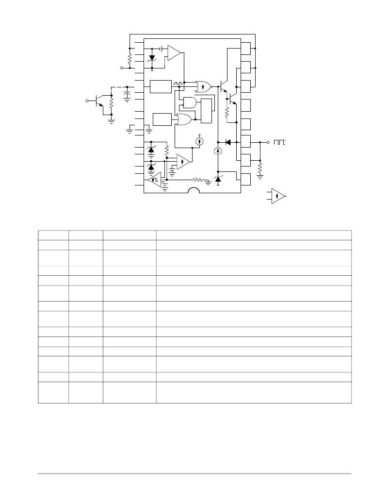
�Figure� 2.� Representative� Block� Diagram�
�PIN� FUNCTION� DESCRIPTION�
�SOIC16�
�1�
�2�
�3�
�4�
�6�
�7�
�8�
�9�
�10,11�
�14,15�
�16�
�5,12,13�
�Exposed�
�Pad�
�DFN18�
�15�
�16�
�17�
�18�
�1�
�3�
�4�
�5�
�6,7,8,9�
�10,11,12,13�
�14�
�2�
�Exposed�
�Pad�
�PIN� NAME�
�LVI� Output�
�Voltage� Feedback� 2�
�Voltage� Feedback� 1�
�GND�
�Timing� Capacitor�
�V� CC�
�I� pk� Sense�
�Drive� Collector�
�Switch� Collector�
�Switch� Emitter�
�Bootstrap� Input�
�No� Connect�
�Exposed� Pad�
�DESCRIPTION�
�This� pin� will� sink� current� when� FB1� and� FB2� are� less� than� the� LVI� threshold� (V� th� ).�
�Connecting� this� pin� to� a� resistor� divider� off� of� the� output� will� regulate� the� application�
�according� to� the� V� out� design� equation� in� Figure� 22.�
�Connecting� this� pin� directly� to� the� output� will� regulate� the� device� to� 5.05� V.�
�Ground� pin� for� all� internal� circuits� and� power� switch.�
�Connect� a� capacitor� to� this� pin� to� set� the� frequency.� The� addition� of� a� parallel� resist-�
�or� will� decrease� the� maximum� duty� cycle� and� increase� the� frequency.�
�Power� pin� for� the� IC.�
�When� (V� CC� ?� V� IPKsense� )� >� 250� mV� the� circuit� resets� the� output� driver� on� a� pulse� by�
�pulse� basis.�
�Voltage� driver� collector�
�Internal� switch� transistor� collector�
�Internal� switch� transistor� emitter�
�Connect� this� pin� to� V� CC� for� operation� at� low� V� CC� levels.� For� some� topologies,� a�
�series� resistor� and� capacitor� can� be� utilized� to� improve� the� converter� efficiency.�
�These� pins� have� no� connection.�
�The� exposed� pad� beneath� the� package� must� be� connected� to� GND� (pin� 4).� Addi-�
�tionally,� using� proper� layout� techniques,� the� exposed� pad� can� greatly� enhance� the�
�power� dissipation� capabilities� of� the� NCP3163.�
�http://onsemi.com�
�2�
�相关PDF资料 |
PDF描述 |
|---|---|
| A9BBG-1408F | FLEX CABLE - AFF14G/AF14/AFF14G |
| NCP1522BUGEVB | EVAL BOARD FOR NCP1522BU |
| RBM11DRTI | CONN EDGECARD 22POS DIP .156 SLD |
| A9CCA-1704E | FLEX CABLE - AFK17A/AE17/AFK17A |
| RCM15DRTH | CONN EDGECARD 30POS DIP .156 SLD |
相关代理商/技术参数 |
参数描述 |
|---|---|
| NCP3163BUCKEVB | 功能描述:BOARD EVAL NCP3163 BUCK RoHS:是 类别:编程器,开发系统 >> 评估板 - DC/DC 与 AC/DC(离线)SMPS 系列:* 产品培训模块:Obsolescence Mitigation Program 标准包装:1 系列:True Shutdown™ 主要目的:DC/DC,步升 输出及类型:1,非隔离 功率 - 输出:- 输出电压:- 电流 - 输出:1A 输入电压:2.5 V ~ 5.5 V 稳压器拓扑结构:升压 频率 - 开关:3MHz 板类型:完全填充 已供物品:板 已用 IC / 零件:MAX8969 |
| NCP3163BUCKGEVB | 功能描述:电源管理IC开发工具 NCP3163 BUCK DEMO BOARD RoHS:否 制造商:Maxim Integrated 产品:Evaluation Kits 类型:Battery Management 工具用于评估:MAX17710GB 输入电压: 输出电压:1.8 V |
| NCP3163INVEVB | 功能描述:电源管理IC开发工具 NCP3163 INVERT DEMO BRD RoHS:否 制造商:Maxim Integrated 产品:Evaluation Kits 类型:Battery Management 工具用于评估:MAX17710GB 输入电压: 输出电压:1.8 V |
| NCP3163INVGEVB | 功能描述:EVAL BOARD FOR NCP3163INV RoHS:是 类别:编程器,开发系统 >> 评估板 - DC/DC 与 AC/DC(离线)SMPS 系列:- 标准包装:1 系列:- 主要目的:DC/DC,步降 输出及类型:1,非隔离 功率 - 输出:- 输出电压:3.3V 电流 - 输出:3A 输入电压:4.5 V ~ 28 V 稳压器拓扑结构:降压 频率 - 开关:250kHz 板类型:完全填充 已供物品:板 已用 IC / 零件:L7981 其它名称:497-12113STEVAL-ISA094V1-ND |
| NCP3163MNR2G | 功能描述:直流/直流开关调节器 DFN 18EG 5X6X.9MM RoHS:否 制造商:International Rectifier 最大输入电压:21 V 开关频率:1.5 MHz 输出电压:0.5 V to 0.86 V 输出电流:4 A 输出端数量: 最大工作温度: 安装风格:SMD/SMT 封装 / 箱体:PQFN 4 x 5 |
发布紧急采购,3分钟左右您将得到回复。