- 您现在的位置:买卖IC网 > PDF目录13633 > NCP3163PWG (ON Semiconductor)IC REG BUCK BOOST INV ADJ 16SOIC PDF资料下载
参数资料
| 型号: | NCP3163PWG |
| 厂商: | ON Semiconductor |
| 文件页数: | 9/20页 |
| 文件大小: | 0K |
| 描述: | IC REG BUCK BOOST INV ADJ 16SOIC |
| 标准包装: | 47 |
| 类型: | 降压(降压),升压(升压),反相 |
| 输出类型: | 可调式 |
| 输出数: | 1 |
| 输出电压: | 可调至 40V |
| 输入电压: | 2.5 V ~ 40 V |
| PWM 型: | 混合物 |
| 频率 - 开关: | 50kHz ~ 300kHz |
| 电流 - 输出: | 3.4A |
| 同步整流器: | 无 |
| 工作温度: | 0°C ~ 70°C |
| 安装类型: | 表面贴装 |
| 封装/外壳: | 16-SOIC(0.295",7.50mm 宽)裸露焊盘 |
| 包装: | 管件 |
| 供应商设备封装: | 16-SOIC W |
�� �
�
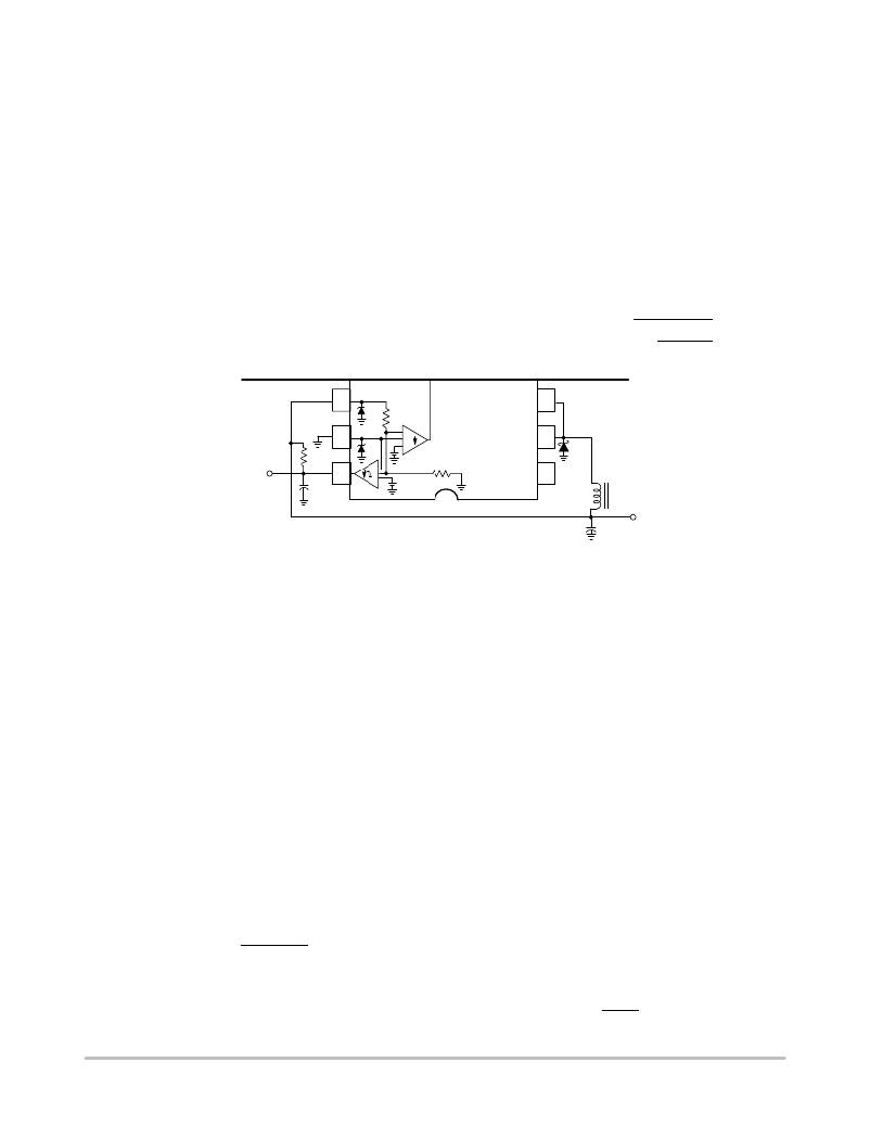
�NCP3163,� NCV3163�
�t� DLY� =� R� LVI� ?� C� DLY� ?� In�
�V� th(MPU)�
�V� out�
�Feedback� and� Low� Voltage� Indicator� Comparators�
�Output� voltage� control� is� established� by� the� Feedback�
�comparator.� The� inverting� input� is� internally� biased� at� 1.25� V�
�and� is� not� pinned� out.� The� converter� output� voltage� is�
�typically� divided� down� with� two� external� resistors� and�
�monitored� by� the� high� impedance� noninverting� input� at� Pin� 2.�
�The� maximum� input� bias� current� is� ±� 0.4� m� A,� which� can� cause�
�an� output� voltage� error� that� is� equal� to� the� product� of� the� input�
�bias� current� and� the� upper� divider� resistance� value.� For�
�applications� that� require� 5.0� V,� the� converter� output� can� be�
�directly� connected� to� the� noninverting� input� at� Pin� 3.� The� high�
�impedance� input,� Pin� 2,� must� be� grounded� to� prevent� noise�
�pickup.� The� internal� resistor� divider� is� set� for� a� nominal�
�voltage� of� 5.05� V.� The� additional� 50� mV� compensates� for� a�
�1.0%� voltage� drop� in� the� cable� and� connector� from� the�
�converter� output� to� the� load.� The� Feedback� comparator’s�
�3�
�output� state� is� controlled� by� the� highest� voltage� applied� to�
�either� of� the� two� noninverting� inputs.�
�The� Low� Voltage� Indicator� (LVI)� comparator� is� designed�
�for� use� as� a� reset� controller� in� microprocessor� ?� based�
�systems.� The� inverting� input� is� internally� biased� at� 1.125� V,�
�which� sets� the� noninverting� input� thresholds� to� 90%� of�
�nominal.� The� LVI� comparator� has� 15� mV� of� hysteresis� to�
�prevent� erratic� reset� operation.� The� Open� Collector� output� is�
�capable� of� sinking� in� excess� of� 6.0� mA� (see� Figure� 13).� An�
�external� resistor� (R� LVI� )� and� capacitor� (C� DLY� )� can� be� used� to�
�program� a� reset� delay� time� (t� DLY� )� by� the� formula� shown�
�below,� where� V� th(MPU)� is� the� microprocessor� reset� input�
�threshold.� Refer� to� Figure� 20.�
�1�
�1� ?�
�14�
�2�
�+�
�+�
�-�
�Feedback�
�Comparator�
�15�
�Low� Voltage�
�Indicator� Output�
�R� LVI�
�C� DLY�
�1�
�LVI�
�+�
�+�
�-�
�1.25� V�
�1.125� V�
�16�
�L�
�(Bottom� View)�
�Figure� 20.� Partial� Application� Schematic� Showing�
�Implementation� of� LVI� Delay� with� R� LVI� and� C� DLY�
�C� O�
�V� out�
�RSC� +�
�RSC(min)� +�
�+� 0.0735� W�
�Current� Limit� Comparator,� Latch� and� Thermal�
�Shutdown�
�With� a� voltage� mode� ripple� converter� operating� under�
�normal� conditions,� output� switch� conduction� is� initiated� by�
�the� oscillator� and� terminated� by� the� Voltage� Feedback�
�comparator.� Abnormal� operating� conditions� occur� when� the�
�converter� output� is� overloaded� or� when� feedback� voltage�
�sensing� is� lost.� Under� these� conditions,� the� Current� Limit�
�comparator� will� protect� the� Output� Switch.�
�The� switch� current� is� converted� to� a� voltage� by� inserting�
�a� fractional� ohm� resistor,� R� SC� ,� in� series� with� V� CC� and� output�
�switch� transistor� Q� 2� .� The� voltage� drop� across� R� SC� is�
�monitored� by� the� Current� Sense� comparator.� If� the� voltage�
�drop� exceeds� 250� mV� with� respect� to� V� CC� ,� the� comparator�
�will� set� the� latch� and� terminate� output� switch� conduction� on�
�a� cycle� ?� by� ?� cycle� basis.� This� Comparator/Latch�
�configuration� ensures� that� the� Output� Switch� has� only� a�
�single� on� ?� time� during� a� given� oscillator� cycle.� The�
�calculation� for� a� value� of� R� SC� is:�
�0.25� V�
�Ipk� (Switch)�
�Figures� 14� and� 15� show� that� the� Current� Sense� comparator�
�threshold� is� tightly� controlled� over� temperature� and� has� a�
�typical� input� bias� current� of� 1.0� m� A.� The� propagation� delay�
�from� the� comparator� input� to� the� Output� Switch� is� typically�
�200� ns.� The� parasitic� inductance� associated� with� R� SC� and� the�
�circuit� layout� should� be� minimized.� This� will� prevent�
�unwanted� voltage� spikes� that� may� falsely� trip� the� Current�
�Limit� comparator.�
�Internal� thermal� shutdown� circuitry� is� provided� to� protect�
�the� IC� in� the� event� that� the� maximum� junction� temperature�
�is� exceeded.� When� activated,� typically� at� 170� °� C,� the� Latch�
�is� forced� into� the� “Set”� state,� disabling� the� Output� Switch.�
�This� feature� is� provided� to� prevent� catastrophic� failures� from�
�accidental� device� overheating.� It� is� not� intended� to� be� used�
�as� a� replacement� for� proper� heatsinking.�
�Driver� and� Output� Switch�
�To� aid� in� system� design� flexibility� and� conversion�
�efficiency,� the� driver� current� source� and� collector,� and�
�output� switch� collector� and� emitter� are� pinned� out�
�separately.� This� allows� the� designer� the� option� of� driving� the�
�output� switch� into� saturation� with� a� selected� force� gain� or�
�driving� it� near� saturation� when� connected� as� a� Darlington.�
�The� output� switch� has� a� typical� current� gain� of� 70� at� 2.5� A�
�and� is� designed� to� switch� a� maximum� of� 40� V� collector� to�
�emitter,� with� up� to� 3.4� A� peak� collector� current.� The�
�minimum� value� for� R� SC� is:�
�0.25 V�
�3.4� A�
�http://onsemi.com�
�9�
�相关PDF资料 |
PDF描述 |
|---|---|
| MAX6733AUTSDD6+T | IC SUPERVISOR MPU W/WD SOT23-6 |
| VE-23J-EX-F2 | CONVERTER MOD DC/DC 36V 75W |
| SCMS5D20-100 | INDUCTOR SMD 10UH 0.903A 100KHZ |
| AVS226M16B12T-F | CAP ALUM 22UF 16V 20% SMD |
| AVS106M35B12T-F | CAP ALUM 10UF 35V 20% SMD |
相关代理商/技术参数 |
参数描述 |
|---|---|
| NCP3163PWR2G | 功能描述:直流/直流开关调节器 ANA 2.5 A STEP UP/ DWN/INV RoHS:否 制造商:International Rectifier 最大输入电压:21 V 开关频率:1.5 MHz 输出电压:0.5 V to 0.86 V 输出电流:4 A 输出端数量: 最大工作温度: 安装风格:SMD/SMT 封装 / 箱体:PQFN 4 x 5 |
| NCP3170ADR2G | 功能描述:直流/直流开关转换器 3A SWITCHING REGULATOR RoHS:否 制造商:STMicroelectronics 最大输入电压:4.5 V 开关频率:1.5 MHz 输出电压:4.6 V 输出电流:250 mA 输出端数量:2 最大工作温度:+ 85 C 安装风格:SMD/SMT |
| NCP3170AGEVB | 功能描述:电源管理IC开发工具 NCP3170ADR2G EVB RoHS:否 制造商:Maxim Integrated 产品:Evaluation Kits 类型:Battery Management 工具用于评估:MAX17710GB 输入电压: 输出电压:1.8 V |
| NCP3170BDR2G | 功能描述:直流/直流开关转换器 3A SWITCHING REGULATOR RoHS:否 制造商:STMicroelectronics 最大输入电压:4.5 V 开关频率:1.5 MHz 输出电压:4.6 V 输出电流:250 mA 输出端数量:2 最大工作温度:+ 85 C 安装风格:SMD/SMT |
| NCP3170BGEVB | 功能描述:电源管理IC开发工具 NCP3170BDR2G EVAL BOARD RoHS:否 制造商:Maxim Integrated 产品:Evaluation Kits 类型:Battery Management 工具用于评估:MAX17710GB 输入电压: 输出电压:1.8 V |
发布紧急采购,3分钟左右您将得到回复。