- 您现在的位置:买卖IC网 > PDF目录13656 > NCP3163PWR2G (ON Semiconductor)IC REG BUCK BOOST INV ADJ 16SOIC PDF资料下载
参数资料
| 型号: | NCP3163PWR2G |
| 厂商: | ON Semiconductor |
| 文件页数: | 11/20页 |
| 文件大小: | 0K |
| 描述: | IC REG BUCK BOOST INV ADJ 16SOIC |
| 标准包装: | 1 |
| 类型: | 降压(降压),升压(升压),反相 |
| 输出类型: | 可调式 |
| 输出数: | 1 |
| 输出电压: | 可调至 40V |
| 输入电压: | 2.5 V ~ 40 V |
| PWM 型: | 混合物 |
| 频率 - 开关: | 50kHz ~ 300kHz |
| 电流 - 输出: | 3.4A |
| 同步整流器: | 无 |
| 工作温度: | 0°C ~ 70°C |
| 安装类型: | 表面贴装 |
| 封装/外壳: | 16-SOIC(0.295",7.50mm 宽)裸露焊盘 |
| 包装: | 剪切带 (CT) |
| 供应商设备封装: | 16-SOIC W |
| 其它名称: | NCP3163PWR2GOSCT |
�� �
�
�NCP3163,� NCV3163�
�Calculation�
�Step� ?� Down�
�Step� ?� Up�
�Voltage� ?� Inverting�
�V� sat�
�in�
�*� V� sat�
�in�
�(See� Notes� 1,2,3)�
�ton�
�toff�
�V�
�in�
�V� out� )� V� F�
�*� V� sat� *� V� out�
�V� out� )� V� F�
�V�
�V�
�in�
�|V out|� )� V F�
�V�
�off�
�t� on�
�)� 1�
�off�
�off�
�t� on�
�)� 1�
�off�
�off�
�t� on�
�)� 1�
�off�
�ton�
�?�
�t�
�t on�
�t�
�?�
�t�
�t on�
�t�
�?�
�t�
�t on�
�t�
�CT�
�32.143 · 10� *� 6�
�f�
�*� 20� @� 10� *� 12�
�32.143 · 10� *� 6�
�f�
�*� 20� @� 10� *� 12�
�32.143 · 10� *� 6�
�f�
�*� 20� @� 10� *� 12�
�off�
�off�
�IL(avg)�
�Iout�
�I� out�
�t on�
�t�
�)� 1�
�I� out�
�t on�
�t�
�)� 1�
�D� I�
�D� I�
�D� I�
�Ipk� (Switch)�
�IL(avg)� )�
�L�
�2�
�IL(avg)� )�
�L�
�2�
�IL(avg)� )�
�L�
�2�
�RSC�
�0.25�
�Ipk� (Switch)�
�0.25�
�Ipk� (Switch)�
�0.25�
�Ipk� (Switch)�
�D� I�
�D� I�
�D� I�
�L�
�V�
�in�
�*� V� sat� *� V� out�
�L�
�t� on�
�V�
�in�
�*� V� sat�
�L�
�t� on�
�V�
�in�
�*� V� sat�
�L�
�t� on�
�O�
�O�
�V� ripple(pp)�
�D� IL�
�1�
�8� ?� CO�
�2�
�)� (ESR)2�
�[�
�t on I out�
�C�
�[�
�t on I out�
�C�
�Vout�
�V�
�ref�
�R2�
�R1�
�)� 1�
�V�
�ref�
�R2�
�R1�
�)� 1�
�V�
�ref�
�R2�
�R1�
�)� 1�
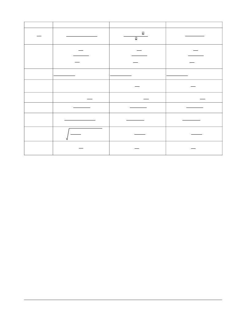
�The� following� Converter� Characteristics� must� be� chosen:�
�V� in� ?�
�V� out� ?�
�I� out� ?�
�D� I� L� ?�
�Nominal� operating� input� voltage.�
�Desired� output� voltage.�
�Desired� output� current.�
�Desired� peak� ?� to� ?� peak� inductor� ripple� current.� For� maximum� output� current� it� is� suggested� that� D� I� L� be� chosen� to� be� less�
�than� 10%� of� the� average� inductor� current� I� L(avg)� .� This� will� help� prevent� I� pk� (Switch)� from� reaching� the� current� limit�
�threshold� set� by� R� SC� .� If� the� design� goal� is� to� use� a� minimum� inductance� value,� let� D� I� L� =� 2(I� L(avg)� ).� This� will�
�proportionally� reduce� converter� output� current� capability.�
�p� ?� Maximum� output� switch� frequency.�
�V� ripple(pp)� ?� Desired� peak� ?� to� ?� peak� output� ripple� voltage.� For� best� performance� the� ripple� voltage� should� be� kept� to� a� low� value�
�since� it� will� directly� affect� line� and� load� regulation.� Capacitor� C� O� should� be� a� low� equivalent� series� resistance� (ESR)�
�electrolytic� designed� for� switching� regulator� applications.�
�NOTES:�
�NOTES:�
�NOTES:�
�NOTES:�
�1.�
�2.�
�3.�
�3.�
�V� sat� ?� Saturation� voltage� of� the� output� switch,� refer� to� Figures� 10� and� 11.�
�V� F� ?� Output� rectifier� forward� voltage� drop.� Typical� value� for� 1N5822� Schottky� barrier� rectifier� is� 0.5� V.�
�The� calculated� t� on� /t� off� must� not� exceed� the� minimum� guaranteed� oscillator� charge� to� discharge� ratio� of� 8,� at� the� minimum�
�operating� input� voltage.�
�Figure� 22.� Design� Equations�
�http://onsemi.com�
�11�
�相关PDF资料 |
PDF描述 |
|---|---|
| MAX16059ATT38+T | IC SUPERVISOR OD 3.8V 6-TDFN |
| MAX16059ATT37+T | IC SUPERVISOR OD 3.7V 6-TDFN |
| MAX16059ATT36+T | IC SUPERVISOR OD 3.6V 6-TDFN |
| MAX16059ATT35+T | IC SUPERVISOR OD 3.5V 6-TDFN |
| MAX16059ATT34+T | IC SUPERVISOR OD 3.4V 6-TDFN |
相关代理商/技术参数 |
参数描述 |
|---|---|
| NCP3170ADR2G | 功能描述:直流/直流开关转换器 3A SWITCHING REGULATOR RoHS:否 制造商:STMicroelectronics 最大输入电压:4.5 V 开关频率:1.5 MHz 输出电压:4.6 V 输出电流:250 mA 输出端数量:2 最大工作温度:+ 85 C 安装风格:SMD/SMT |
| NCP3170AGEVB | 功能描述:电源管理IC开发工具 NCP3170ADR2G EVB RoHS:否 制造商:Maxim Integrated 产品:Evaluation Kits 类型:Battery Management 工具用于评估:MAX17710GB 输入电压: 输出电压:1.8 V |
| NCP3170BDR2G | 功能描述:直流/直流开关转换器 3A SWITCHING REGULATOR RoHS:否 制造商:STMicroelectronics 最大输入电压:4.5 V 开关频率:1.5 MHz 输出电压:4.6 V 输出电流:250 mA 输出端数量:2 最大工作温度:+ 85 C 安装风格:SMD/SMT |
| NCP3170BGEVB | 功能描述:电源管理IC开发工具 NCP3170BDR2G EVAL BOARD RoHS:否 制造商:Maxim Integrated 产品:Evaluation Kits 类型:Battery Management 工具用于评估:MAX17710GB 输入电压: 输出电压:1.8 V |
| NCP317BTG | 功能描述:稳压二极管 ANA ADJUST OUT VREG 1.5A RoHS:否 制造商:Vishay Semiconductors 齐纳电压:12 V 电压容差:5 % 电压温度系数:0.075 % / K 齐纳电流: 功率耗散:3 W 最大反向漏泄电流:3 uA 最大齐纳阻抗:7 Ohms 最大工作温度:+ 150 C 安装风格:SMD/SMT 封装 / 箱体:DO-214AC 封装:Reel |
发布紧急采购,3分钟左右您将得到回复。