- 您现在的位置:买卖IC网 > Datasheet目录346 > NCP3418DR2 (ON Semiconductor)IC MOSFET DRIVER DUAL 12V 8-SOIC Datasheet资料下载
参数资料
| 型号: | NCP3418DR2 |
| 厂商: | ON Semiconductor |
| 文件页数: | 3/9页 |
| 文件大小: | 0K |
| 描述: | IC MOSFET DRIVER DUAL 12V 8-SOIC |
| 产品变化通告: | Product Discontinuation 31/Mar/2005 |
| 标准包装: | 1 |
| 配置: | 高端和低端,同步 |
| 输入类型: | PWM |
| 延迟时间: | 30ns |
| 电流 - 峰: | 1.5A |
| 配置数: | 1 |
| 输出数: | 2 |
| 高端电压 - 最大(自引导启动): | 30V |
| 电源电压: | 4.6 V ~ 13.2 V |
| 工作温度: | 0°C ~ 85°C |
| 安装类型: | 表面贴装 |
| 封装/外壳: | 8-SOIC(0.154",3.90mm 宽) |
| 供应商设备封装: | 8-SOICN |
| 包装: | 剪切带 (CT) |
| 其它名称: | NCP3418DR2CT |
�� �
�
�NCP3418,� NCP3418A�
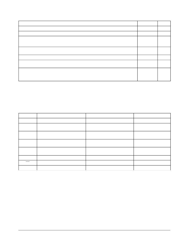
�MAXIMUM� RATINGS�
�Operating� Ambient� Temperature,� T� A�
�Operating� Junction� Temperature,� T� J� (Note� 1)�
�Package� Thermal� Resistance:� SO--8�
�Junction--to--Case,� R� θ� JC�
�Junction--to--Ambient,� R� θ� JA� (2--Layer� Board)�
�Package� Thermal� Resistance:� SO--8� EP�
�Junction--to--Ambient,� R� θ� JA� (Note� 2)�
�Storage� Temperature� Range,� T� S�
�Rating�
�Value�
�0� to� 85�
�0� to� 150�
�45�
�123�
�50�
�--65� to� 150�
�Unit�
�°� C�
�°� C�
�°� C/W�
�°� C/W�
�°� C/W�
�°� C�
�Lead� Temperature� Soldering� (10� sec):� Reflow� (SMD� styles� only)�
�JEDEC� Moisture� Sensitivity� Level�
�Standard� (Note� 3)�
�Lead� Free� (Note� 4)�
�SO--8� (240� peak� profile)�
�SO--8� (260� peak� profile)�
�SO--8� EP� (240� peak� profile)�
�SO--8� EP� (260� peak� profile)�
�240� peak�
�260� peak�
�1�
�1�
�1�
�3�
�°� C�
�--�
�Stresses� exceeding� Maximum� Ratings� may� damage� the� device.� Maximum� Ratings� are� stress� ratings� only.� Functional� operation� above� the�
�Recommended� Operating� Conditions� is� not� implied.� Extended� exposure� to� stresses� above� the� Recommended� Operating� Conditions� may� affect�
�device� reliability.�
�1.� Internally� limited� by� thermal� shutdown,� 150� °� C� min.�
�2.� Rating� applies� when� soldered� to� an� appropriate� thermal� area� on� the� PCB.�
�3.� 60� --� 180� seconds� minimum� above� 183� °� C.�
�4.� 60� --� 180� seconds� minimum� above� 237� °� C.�
�NOTE:� This� device� is� ESD� sensitive.� Use� standard� ESD� precautions� when� handling.�
�MAXIMUM� RATINGS�
�Pin� Symbol�
�V� CC�
�BST�
�SW�
�DRVH�
�DRVL�
�IN�
�OD�
�PGND�
�Pin� Name�
�Main� Supply� Voltage� Input�
�Bootstrap� Supply� Voltage� Input�
�Switching� Node�
�(Bootstrap� Supply� Return)�
�High--Side� Driver� Output�
�Low--Side� Driver� Output�
�DRVH� and� DRVL� Control� Input�
�Output� Disable�
�Ground�
�V� MAX�
�15� V�
�30� V� wrt/PGND�
�35� V� ≤� 50� ns� wrt/PGND,� 15� V� wrt/SW�
�30� V�
�BST� +� 0.3� V�
�35� V� ≤� 50� ns� wrt/PGND,� 15� V� wrt/SW�
�V� CC� +� 0.3� V�
�V� CC� +� 0.3� V�
�V� CC� +� 0.3� V�
�0V�
�V� MIN�
�--0.3� V�
�--0.3� V� wrt/SW�
�--1.0� V� DC�
�--10� V<� 200� ns�
�--0.3� V� wrt/SW�
�--0.3� V� DC�
�--2.0� V� <� 200� ns�
�--0.3� V�
�--0.3� V�
�0V�
�NOTE:�
�All� voltages� are� with� respect� to� PGND� except� where� noted.�
�http://onsemi.com�
�3�
�相关PDF资料 |
PDF描述 |
|---|---|
| NCP3420DR2G | IC MOSFET DRIVER DUAL 12V 8-SOIC |
| NCP3488DR2G | IC MOSFET DRVR DUAL 12V 8-SOIC |
| NCP5007SNT1 | IC LED DRIVR WHT COMPACT 5TSOP |
| NCP5008DMR2 | IC LED DRVR WHT BCKLT 10MICROSMD |
| NCP5010FCT1G | IC LED DRVR WHT BCKLT 8-FLIPCHIP |
相关代理商/技术参数 |
参数描述 |
|---|---|
| NCP3418DR2G | 功能描述:功率驱动器IC ANA 12V MOSFET DR RoHS:否 制造商:Micrel 产品:MOSFET Gate Drivers 类型:Low Cost High or Low Side MOSFET Driver 上升时间: 下降时间: 电源电压-最大:30 V 电源电压-最小:2.75 V 电源电流: 最大功率耗散: 最大工作温度:+ 85 C 安装风格:SMD/SMT 封装 / 箱体:SOIC-8 封装:Tube |
| NCP3418PDR2 | 制造商:Rochester Electronics LLC 功能描述:- Bulk |
| NCP341MUTBG | 制造商:ON Semiconductor 功能描述:Controlled Load Switch Soft-Start |
| NCP3420DR2G | 功能描述:功率驱动器IC TSMC 12V FET DRVR RoHS:否 制造商:Micrel 产品:MOSFET Gate Drivers 类型:Low Cost High or Low Side MOSFET Driver 上升时间: 下降时间: 电源电压-最大:30 V 电源电压-最小:2.75 V 电源电流: 最大功率耗散: 最大工作温度:+ 85 C 安装风格:SMD/SMT 封装 / 箱体:SOIC-8 封装:Tube |
| NCP3420DR2G-CUT TAPE | 制造商:ON 功能描述:NCP Series 1.8 Ohm 13.2 V Surface Mount MOSFET Driver with Dual Outputs - SOIC-8 |
发布紧急采购,3分钟左右您将得到回复。