参数资料
| 型号: | NCP5201MNR2G |
| 厂商: | ON Semiconductor |
| 文件页数: | 4/9页 |
| 文件大小: | 0K |
| 描述: | IC CTRLR PWR DDR DUAL 5X6 18-DFN |
| 产品变化通告: | Product Discontinuation 01/Oct/2008 |
| 标准包装: | 2,500 |
| 应用: | 控制器,DDR |
| 输入电压: | 9.2 V ~ 12 V |
| 输出数: | 2 |
| 工作温度: | 0°C ~ 70°C |
| 安装类型: | 表面贴装 |
| 封装/外壳: | 18-VFDFN 裸露焊盘 |
| 供应商设备封装: | 18-DFN(5x6) |
| 包装: | 带卷 (TR) |
| 其它名称: | NCP5201MNR2GOS |
�� �
�
�NCP5201�
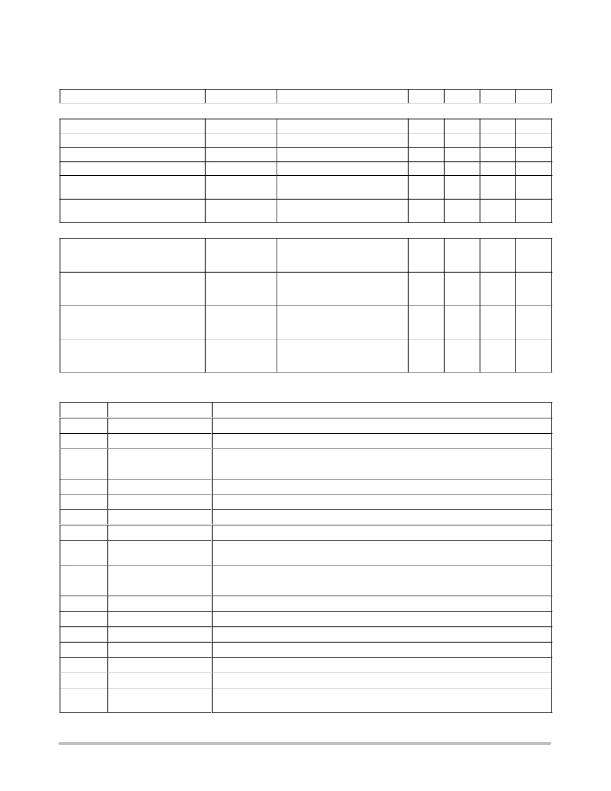
�ELECTRICAL� CHARACTERISTICS� (VSTBY� =� 5.0� V,� VCC� =� 12� V,� T� A� =� 0� to� 70� °� C,� L2� =� 1.7� m� H,� COUT� =� 3770� m� F,� COUT2� =� 220� m� F,�
�RL1� =� 100� k� W� ,� R7� =� 1.0� k� W� ,� R10� =� 1.0� k,� R12� =� 20� k� W� ,� R6� =� 16� W� ,� C12� =� 3.0� nF,� C11� =� 6.0� nF,� C10� =� 80� nF,� for� min/max� values� unless�
�otherwise� noted)�
�Characteristic�
�Symbol�
�Test� Conditions�
�Min�
�Typ�
�Max�
�Unit�
�CONTROL� SECTION�
�S3_EN� Pin� Threshold� HIGH�
�S3_EN� Pin� Threshold� LOW�
�S3_EN� Pin� Input� Current�
�PWRGD� Pin� ON� Resistance�
�PWRGD� Pin� OFF� Current�
�?�
�?�
�?�
�?�
�?�
�S3_EN_H�
�S3_EN_L�
�IIN_EN�
�PWRGD_R�
�PWRGD_�
�1.4�
�?�
�?�
�?�
�?�
�?�
�?�
�?�
�?�
�?�
�?�
�0.5�
�0.5�
�80�
�1.0�
�V�
�V�
�m� A�
�W�
�m� A�
�LEAK�
�PWRGD� LOW?to?HIGH� Hold� Time,�
�?�
�thold�
�?�
�?�
�200�
�m� s�
�For� S3� to� S0� or� S5� to� S0�
�GATE� DRIVERS�
�TGDDQ� Gate� Pull?HIGH� Resistance�
�VCC� =� 12� V,�
�RH_TG�
�?�
�3.0�
�?�
�W�
�V(TGDDQ)� =� 11�
�V�
�TGDDQ� Gate� Pull?LOW� Resistance�
�VCC� =� 12� V,�
�RL_TG�
�?�
�2.5�
�?�
�W�
�V(TGDDQ)� =� 1.0�
�V�
�BGDDQ� Gate� Pull?HIGH� Resistance�
�VCC� =� 12� V,�
�RH_BG�
�?�
�3.0�
�?�
�W�
�V(BGDDQ)� =� 11�
�V�
�BGDDQ� Gate� Pull?LOW� Resistance�
�VCC� =� 12� V,�
�RL_BG�
�?�
�1.3�
�?�
�W�
�V(BGDDQ)� =� 1.0�
�V�
�PIN� DESCRIPTION�
�Pin� No.�
�1�
�2�
�3�
�4�
�5,� 6�
�7�
�8�
�9�
�10�
�11�
�12�
�13�
�14�
�15�
�16�
�17�
�18�
�19�
�Symbol�
�FBDDQ�
�FBVTT�
�PGND�
�VSTBY�
�VTT�
�OCDDQ�
�VDDQ�
�NC�
�PWRGD�
�S3_EN�
�AGND�
�SDDQ�
�BGDDQ�
�TGDDQ�
�VCC�
�COMP�
�SS�
�TH_PAD�
�Description�
�VDDQ� feedback� pin� for� closed� loop� regulation.�
�VTT� regulator� sense� voltage.�
�Power� ground.�
�5� V� Standby� input� voltage.�
�VTT� regulator� output.�
�Overcurrent� sense� and� program� input� for� the� VDDQ� high?side� FET.�
�Reference� input� and� power� stage� input� for� VTT� regulator.�
�Not� connected.�
�Open� drain� status� output.� High� impedance� when� the� product� is� operating� in� S0� state� and� both�
�DDQ� and� VTT� regulators� are� in� compliance.�
�S3� mode� enable� input.� High� to� enable.�
�Analog� ground� connection� and� remote� ground� sense.�
�Inductor� driven� node� and� current� limit� sense� input.�
�Gate� driver� output,� VDDQ� Low?Side� N?Channel� Power� FET.� Active� during� S0� mode.�
�Gate� driver� output,� VDDQ� High?Side� N?Channel� Power� FET.� Active� during� S0� mode.�
�12� Volt� input� supply.� This� voltage� is� monitored� by� power� good� circuitry� for� mode� selection.�
�VDDQ� error� amplifier� compensation� node.�
�Soft?start� capacitor� connection� to� ground.�
�Copper� pad� on� bottom� of� IC� used� for� heatsinking.� This� pin� should� be� connected� to� the� ground�
�plane� under� the� IC.�
�http://onsemi.com�
�4�
�相关PDF资料 |
PDF描述 |
|---|---|
| X4645V8I | IC SUPERVISOR CPU 64K EE 8-TSSOP |
| GSA28DRMI | CONN EDGECARD 56POS .125 SQ WW |
| GSC44DRES-S93 | CONN EDGECARD 88POS .100 EYELET |
| TC1073-3.6VCH713 | IC REG LDO 3.6V .1A SOT23A-6 |
| NCP4523G1T1G | IC REG LDO CMOS 3CH FOR RF 8SSOP |
相关代理商/技术参数 |
参数描述 |
|---|---|
| NCP5203 | 制造商:ONSEMI 制造商全称:ON Semiconductor 功能描述:2-in-1 DDR Power Controller |
| NCP5203/D | 制造商:未知厂家 制造商全称:未知厂家 功能描述:2-in-1 DDR Power Controller |
| NCP5203MNR2 | 功能描述:DC/DC 开关控制器 2-in-1 DDR Power RoHS:否 制造商:Texas Instruments 输入电压:6 V to 100 V 开关频率: 输出电压:1.215 V to 80 V 输出电流:3.5 A 输出端数量:1 最大工作温度:+ 125 C 安装风格: 封装 / 箱体:CPAK |
| NCP5203MNR2G | 功能描述:DC/DC 开关控制器 2-in-1 DDR Power RoHS:否 制造商:Texas Instruments 输入电压:6 V to 100 V 开关频率: 输出电压:1.215 V to 80 V 输出电流:3.5 A 输出端数量:1 最大工作温度:+ 125 C 安装风格: 封装 / 箱体:CPAK |
| NCP5208 | 制造商:ONSEMI 制造商全称:ON Semiconductor 功能描述:DDR−I/II Termination Regulator |
发布紧急采购,3分钟左右您将得到回复。