参数资料
| 型号: | NCP5203MNR2G |
| 厂商: | ON Semiconductor |
| 文件页数: | 4/10页 |
| 文件大小: | 0K |
| 描述: | IC CTRLR PWR DDR DUAL 5X6 18-DFN |
| 产品变化通告: | Product Discontinuation 01/Oct/2008 |
| 标准包装: | 2,500 |
| 应用: | 控制器,DDR |
| 输入电压: | 4.5 V ~ 5.5 V |
| 输出数: | 2 |
| 工作温度: | 0°C ~ 70°C |
| 安装类型: | 表面贴装 |
| 封装/外壳: | 18-VFDFN 裸露焊盘 |
| 供应商设备封装: | 18-DFN(5x6) |
| 包装: | 带卷 (TR) |
| 其它名称: | NCP5203MNR2GOS |
�� �
�
�NCP5203�
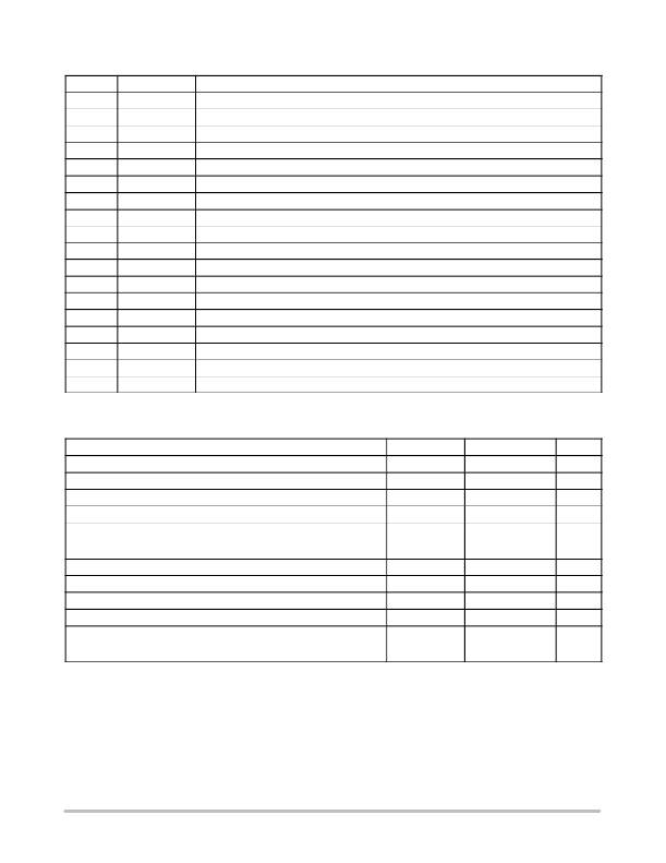
�PIN� FUNCTION� DESCRIPTION�
�Pin� No.�
�1�
�2�
�3�
�4�
�5�
�6�
�7�
�8�
�9�
�10�
�11�
�12�
�13�
�14�
�15�
�16�
�17�
�18�
�Symbol�
�VDDQEN�
�VTTEN�
�PGOOD�
�REFSNS�
�FBVTT�
�AGND�
�SS�
�COMP�
�FBDDQ�
�OCDDQ�
�SWDDQ�
�5VDUAL�
�TGDDQ�
�BGDDQ�
�BST�
�PGND�
�VTT�
�VDDQ�
�Description�
�VDDQ� regulator� enable� input.� Active� high.�
�VTT� regulator� enable� input.� Active� high.�
�Power� good� signal� open?drain� output.�
�Reference� voltage� input� of� VTT� regulator.�
�VTT� regulator� feedback� pin� for� closed� loop� regulation.�
�Analog� ground� connection� and� remote� ground� sense.�
�Soft?start� capacitor� connection� to� ground.�
�VDDQ� error� amplifier� compensation� node.�
�VDDQ� regulator� feedback� pin� for� closed� loop� regulation.�
�Overcurrent� sense� and� program� input� for� the� high?side� FET� of� VDDQ� regulator.�
�VDDQ� regulator� inductor� driven� node� and� current� limit� sense� input.�
�5VDUAL� supply� input.�
�Gate� driver� output� for� DDQ� regulator� high?side� N?Channel� power� FET.�
�Gate� driver� output� for� DDQ� regulator� low?side� N?Channel� power� FET.�
�Supply� input� of� VDDQ� regulator� and� 5� V� boost� capacitor� connection.�
�Power� ground.�
�VTT� regulator� output.�
�Power� input� for� VTT� regulator.�
�MAXIMUM� RATINGS� (Note� 1)�
�Rating�
�Power� Supply� Voltage� (Pin� 12,� 18)�
�Gate� Drive� Supply/Output� Voltage� (Pin� 13,� 14,� 15)�
�Switch� DDQ� (Pin� 11)�
�Input/Output� Pins� (Pin� 1,� 2,� 7;� 4,� 5,� 17;� 3,� 8,� 9,� 10)�
�Thermal� Characteristics�
�QFN?18� Plastic� Package�
�Thermal� Resistance� Junction?to?Ambient�
�Operating� Junction� Temperature� Range�
�Operating� Ambient� Temperature� Range�
�Storage� Temperature� Range�
�Moisture� Sensitivity� Level�
�Symbol�
�5VDUAL�
�VBST,� Vg�
�SWDDQ�
�V� IO�
�R� q� JA�
�T� J�
�T� A�
�T� stg�
�MSL�
�Value�
�?0.3,� 6.5�
�?0.3,� 14�
�?1.0,� 5VDUAL�
�?0.3,� 6.5�
�35�
�0� to� +150�
�0� to� +70�
�?55� to� +150�
�2.0�
�Unit�
�V�
�V�
�V�
�V�
�°� C/W�
�°� C�
�°� C�
�°� C�
�?�
�Electro� Static� Discharge� (ESD)�
�Human� Body� Model�
�Machine� Model�
�HBM�
�MM�
�2.0�
�200�
�kV�
�V�
�Maximum� ratings� are� those� values� beyond� which� device� damage� can� occur.� Maximum� ratings� applied� to� the� device� are� individual� stress� limit� values�
�(not� normal� operating� conditions)� and� are� not� valid� simultaneously.� If� these� limits� are� exceeded,� device� functional� operation� is� not� implied,� damage�
�may� occur� and� reliability� may� be� affected.�
�1.� All� voltages� are� with� respect� to� AGND� (Pin� 6)� and� PGND� (Pin� 16).�
�http://onsemi.com�
�4�
�相关PDF资料 |
PDF描述 |
|---|---|
| NCP5208DR2G | IC REG TERM DDR-I/II 1.7V 8SOIC |
| NCP5210MNR2G | IC CTLR PWM/DDR DUAL BUCK 20-DFN |
| NCP5211BDR2G | IC REG CTRLR BUCK PWM 14-SOIC |
| NCP5212AMNTXG | IC REG CTRLR BUCK PWM 16-QFN |
| NCP5214AMNR2G | IC CTLR NOTEBOOK DDR PWR 22-DFN |
相关代理商/技术参数 |
参数描述 |
|---|---|
| NCP5208 | 制造商:ONSEMI 制造商全称:ON Semiconductor 功能描述:DDR−I/II Termination Regulator |
| NCP5208/D | 制造商:ONSEMI 制造商全称:ON Semiconductor 功能描述:DDR-I/II Termination Regulator |
| NCP5208_06 | 制造商:ONSEMI 制造商全称:ON Semiconductor 功能描述:DDR−I/II Termination Regulator |
| NCP5208DR2 | 功能描述:线性稳压器 - 标准 DDR-I/II Termination RoHS:否 制造商:STMicroelectronics 输出类型: 极性: 输出电压:1.8 V 输出电流:150 mA 负载调节: 最大输入电压:5.5 V 线路调整率: 最大工作温度:+ 125 C 安装风格:SMD/SMT 封装 / 箱体:SOT-323-5L |
| NCP5208DR2G | 功能描述:线性稳压器 - 标准 DDR-I/II Termination RoHS:否 制造商:STMicroelectronics 输出类型: 极性: 输出电压:1.8 V 输出电流:150 mA 负载调节: 最大输入电压:5.5 V 线路调整率: 最大工作温度:+ 125 C 安装风格:SMD/SMT 封装 / 箱体:SOT-323-5L |
发布紧急采购,3分钟左右您将得到回复。