参数资料
| 型号: | NCP5212AMNTXG |
| 厂商: | ON Semiconductor |
| 文件页数: | 13/19页 |
| 文件大小: | 0K |
| 描述: | IC REG CTRLR BUCK PWM 16-QFN |
| 标准包装: | 1 |
| PWM 型: | 电流/电压模式 |
| 输出数: | 1 |
| 频率 - 最大: | 330kHz |
| 电源电压: | 4.5 V ~ 27 V |
| 降压: | 是 |
| 升压: | 无 |
| 回扫: | 无 |
| 反相: | 无 |
| 倍增器: | 无 |
| 除法器: | 无 |
| Cuk: | 无 |
| 隔离: | 无 |
| 工作温度: | -40°C ~ 85°C |
| 封装/外壳: | 16-VQFN 裸露焊盘 |
| 包装: | 标准包装 |
| 其它名称: | NCP5212AMNTXGOSDKR |
�� �
�
�NCP5212A,� NCP5212T�
�Once� the� large� transient� occurs,� the� COMP� signal� may� be�
�large� enough� to� exceed� the� threshold� and� then� TRE� “flag”�
�signal� will� be� asserted� in� a� short� period� which� is� typically�
�around� one� normal� switching� cycle.� In� this� short� period,� the�
�controller� will� be� running� at� high� frequency� and� hence� has�
�faster� response.� After� that� the� controller� comes� back� to�
�normal� switching� frequency� operation.� We� can� program� the�
�internal� TRE� threshold� (TRE_TH).� For� detail� please� see� the�
�electrical� table� of� “TRE� Setting”� section.� Basically,� the�
�recommend� internal� TRE� threshold� value� is� around� 1.5�
�times� of� peak� ?� to� ?� peak� value� of� the� COMP� signal� at� CCM�
�operation.� The� higher� the� internal� TRE_TH,� the� lower�
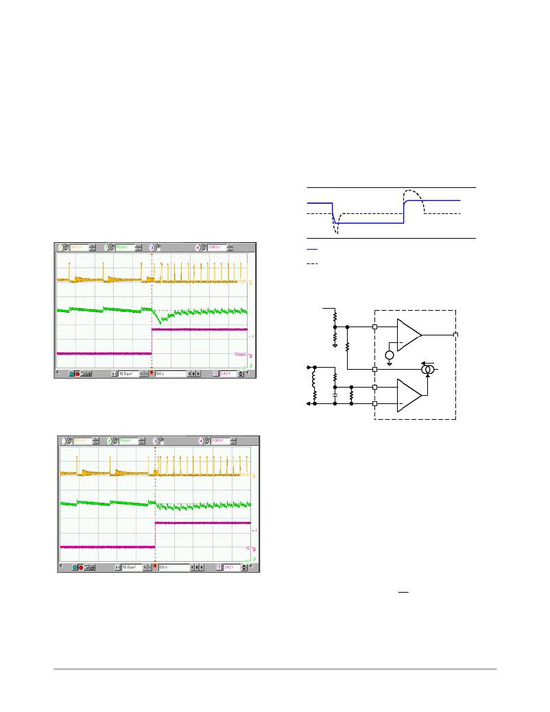
�Adaptive� Voltage� Positioning� (AVP)�
�For� applications� with� fast� transient� currents,� adaptive�
�voltage� positioning� can� reduce� peak� ?� to� ?� peak� output� voltage�
�deviations� due� to� load� transients.� With� the� use� of� AVP,� the�
�output� voltage� allows� to� have� some� controlled� sag� when� load�
�current� is� applied.� Upon� removal� of� the� load,� the� output�
�voltage� returns� no� higher� than� the� original� level,� just�
�allowing� one� output� transient� peak� to� be� cancelled� over� a�
�load� step� up� and� release� cycle.� The� amount� of� AVP� is�
�adjustable.�
�The� behaviors� of� the� V� o� waveforms� with� or� without� AVP�
�are� depicted� at� Figure� 20.�
�sensitivity� to� load� transient.� The� TRE� function� can� be�
�disable� by� setting� the� Rtre� which� is� connecting� to� DL/TRE�
�pin� to� less� than� 25� k� W� .� For� system� component� saving,� it� is�
�usually� set� as� default� value,� that� is,� Rtre� is� open� (� w� 75� k� W� )�
�and� internal� TRE_TH� is� 300� mV� typical.�
�Vo� With� AVP�
�Vo� Without� AVP�
�Figure� 20.� Adaptive� Voltage� Positioning�
�Vo�
�Rt�
�Rb�
�FB�
�+�
�COMP�
�+� Vref�
�Rocp�
�IDRP/OCP�
�?�
�IDRP�
�L�
�Rs1�
�CS+�
�Top� to� Bottom� SWN,� Vo,� Transient� Signal�
�Figure� 18.� Transient� Response� with� TRE� Disable�
�DCR�
�Cs�
�Rs2�
�CS� ?�
�+�
�Gi�
�Figure� 21.� Configuration� for� AVP� Function�
�The� Figure� 21� shows� how� to� realize� the� AVP� function.� A�
�current� path� is� connecting� to� the� FB� pin� via� Rocp� resistor.�
�Rocp� is� not� actually� for� AVP� function,� indeed,� Rocp� is� used�
�for� OCP� threshold� value� programming.� The� IDRP/OCP� pin�
�has� dual� functions:� OCP� programming� and� AVP.� At� the�
�IDRP/OCP� pin,� conceptually� there� is� a� current� source� which�
�is� modulated� by� current� sensing� amplifier.�
�The� output� voltage� V� o� with� AVP� is:�
�V� O� +� V� O� 0� *� I� O� *� R� LL�
�(eq.� 1)�
�V� O� 0� +� 1� )�
�*� V� ref�
�Rt�
�Top� to� Bottom� SWN,� Vo,� Transient� Signal�
�Figure� 19.� Transient� Response� with� TRE� Enable�
�Where� I� o� is� the� load� current,� no� load� output� voltage� V� o� 0� is�
�set� by� the� external� divider� that� is:�
�(eq.� 2)�
�Rb�
�http://onsemi.com�
�13�
�相关PDF资料 |
PDF描述 |
|---|---|
| NCP5214AMNR2G | IC CTLR NOTEBOOK DDR PWR 22-DFN |
| NCP5214MNR2G | IC CTLR NOTEBOOK DDR PWR 22-DFN |
| NCP5215MNR2G | IC CTLR SYNC BUCK DUAL 40-QFN |
| NCP5217AMNTXG | IC REG CTRLR BUCK PWM 14-QFN |
| NCP5218MNR2G | IC DDR PWR CTLR 2IN2 NTBK 22-DFN |
相关代理商/技术参数 |
参数描述 |
|---|---|
| NCP5212T | 制造商:ONSEMI 制造商全称:ON Semiconductor 功能描述:Single Synchronous Step-Down Controller |
| NCP5212TMNTXG | 功能描述:DC/DC 开关控制器 SYNC STEP DOWN CONTROLLER RoHS:否 制造商:Texas Instruments 输入电压:6 V to 100 V 开关频率: 输出电压:1.215 V to 80 V 输出电流:3.5 A 输出端数量:1 最大工作温度:+ 125 C 安装风格: 封装 / 箱体:CPAK |
| NCP5214 | 制造商:ONSEMI 制造商全称:ON Semiconductor 功能描述:2-in-1 Notebook DDR Power Controller |
| NCP5214A | 制造商:ONSEMI 制造商全称:ON Semiconductor 功能描述:2−in−1 Notebook DDR Power Controller |
| NCP5214AMNR2G | 功能描述:DC/DC 开关控制器 OSPI 2 IN 1 NTEBOOK RoHS:否 制造商:Texas Instruments 输入电压:6 V to 100 V 开关频率: 输出电压:1.215 V to 80 V 输出电流:3.5 A 输出端数量:1 最大工作温度:+ 125 C 安装风格: 封装 / 箱体:CPAK |
发布紧急采购,3分钟左右您将得到回复。