- 您现在的位置:买卖IC网 > PDF目录20599 > NCP5304PG (ON Semiconductor)IC DRIVER HI/LOW SIDE HV 8-PDIP PDF资料下载
参数资料
| 型号: | NCP5304PG |
| 厂商: | ON Semiconductor |
| 文件页数: | 4/16页 |
| 文件大小: | 0K |
| 描述: | IC DRIVER HI/LOW SIDE HV 8-PDIP |
| 标准包装: | 50 |
| 配置: | 半桥 |
| 输入类型: | 非反相 |
| 延迟时间: | 100ns |
| 电流 - 峰: | 250mA |
| 配置数: | 1 |
| 输出数: | 2 |
| 高端电压 - 最大(自引导启动): | 600V |
| 电源电压: | 10 V ~ 20 V |
| 工作温度: | -40°C ~ 125°C |
| 安装类型: | 通孔 |
| 封装/外壳: | 8-DIP(0.300",7.62mm) |
| 供应商设备封装: | 8-PDIP |
| 包装: | 管件 |
��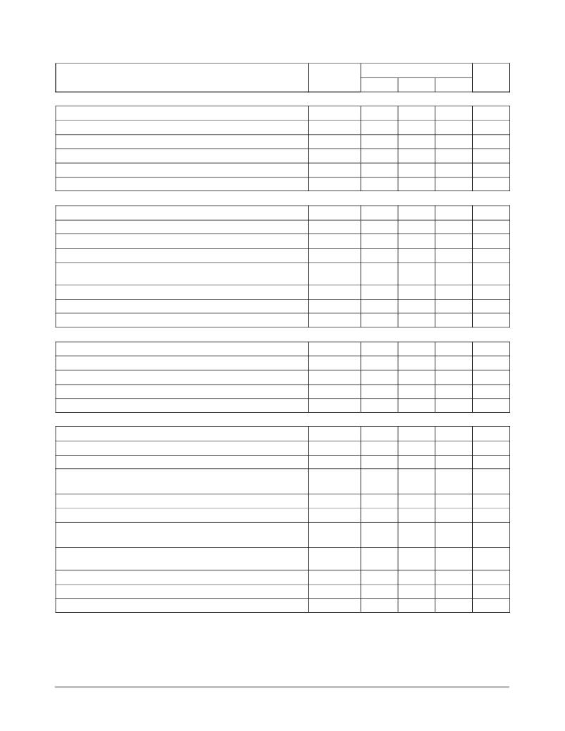 �
�
�NCP5304�
�ELECTRICAL CHARACTERISTIC� (V� CC� = V� boot� = 15 V, V� GND� = V� bridge� ,� ?� 40� °� C < T� J� < 12� 5� °� C,� Outputs� loaded� with� 1� nF)�
�T� J� ?� 40� °� C� to� 125� °� C�
�Rating�
�Symbol�
�Min�
�Typ�
�Max�
�Units�
�OUTPUT� SECTION�
�Output� high� short� circuit� pulsed� current� V� DRV� =� 0� V,� PW� v� 10� m� s� (Note� 1)�
�Output� low� short� circuit� pulsed� current� V� DRV� =� V� CC� ,� PW� v� 10� m� s� (Note� 1)�
�Output� resistor� (Typical� value� @� 25� °� C)� Source�
�Output� resistor� (Typical� value� @� 25� °� C)� Sink�
�High� level� output� voltage,� V� BIAS� ?� V� DRV_XX� @� I� DRV_XX� =� 20� mA�
�Low� level� output� voltage� V� DRV_XX� @� I� DRV_XX� =� 20� mA�
�I� DRVsource�
�I� DRVsink�
�R� OH�
�R� OL�
�V� DRV_H�
�V� DRV_L�
�?�
�?�
�?�
�?�
�?�
�?�
�250�
�500�
�30�
�10�
�0.7�
�0.2�
�?�
�?�
�60�
�20�
�1.6�
�0.6�
�mA�
�mA�
�W�
�W�
�V�
�V�
�DYNAMIC� OUTPUT� SECTION�
�Turn� ?� on� propagation� delay� (Vbridge� =� 0� V)�
�Turn� ?� off� propagation� delay� (Vbridge� =� 0� V� or� 50� V)� (Note� 2)�
�Output� voltage� rise� time� (from� 10%� to� 90%� @� V� CC� =� 15� V)� with� 1� nF� load�
�Output� voltage� fall� time� (from� 90%� to� 10%� @V� CC� =� 15� V)� with� 1� nF� load�
�Propagation� delay� matching� between� the� High� side� and� the� Low� side�
�@� 25� °� C� (Note� 3)�
�Internal� fixed� dead� time� (Note� 4)�
�Minimum� input� width� that� changes� the� output�
�Maximum� input� width� that� does� not� change� the� output�
�t� ON�
�t� OFF�
�tr�
�tf�
�D� t�
�DT�
�t� PW1�
�t� PW2�
�?�
�?�
�?�
�?�
�?�
�65�
�?�
�20�
�100�
�100�
�85�
�35�
�20�
�100�
�?�
�?�
�170�
�170�
�160�
�75�
�35�
�190�
�50�
�?�
�ns�
�ns�
�ns�
�ns�
�ns�
�ns�
�ns�
�ns�
�INPUT� SECTION�
�Low� level� input� voltage� threshold�
�Input� pull� ?� down� resistor� (V� IN� <� 0.5� V)�
�High� level� input� voltage� threshold�
�Logic� “1”� input� bias� current� @� V� IN_XX� =� 5� V� @� 25� °� C�
�Logic� “0”� input� bias� current� @� V� IN_XX� =� 0� V� @� 25� °� C�
�V� IN�
�R� IN�
�V� IN�
�I� IN+�
�I� IN� ?�
�?�
�?�
�2.3�
�?�
�?�
�?�
�200�
�?�
�5�
�?�
�0.8�
�?�
�?�
�25�
�2.0�
�V�
�k� W�
�V�
�m� A�
�m� A�
�SUPPLY� SECTION�
�V� CC� UV� Start� ?� up� voltage� threshold�
�V� CC� UV� Shut� ?� down� voltage� threshold�
�Hysteresis� on� V� CC�
�Vboot� Start� ?� up� voltage� threshold� reference� to� bridge� pin�
�VCC_stup�
�VCC_shtdwn�
�VCC_hyst�
�Vboot_stup�
�8.0�
�7.3�
�0.3�
�8.0�
�8.9�
�8.2�
�0.7�
�8.9�
�9.9�
�9.1�
�?�
�9.9�
�V�
�V�
�V�
�V�
�(Vboot_stup� =� Vboot� ?� Vbridge)�
�Vboot� UV� Shut� ?� down� voltage� threshold�
�Hysteresis� on� Vboot�
�Leakage� current� on� high� voltage� pins� to� GND�
�Vboot_shtdwn�
�Vboot_shtdwn�
�I� HV_LEAK�
�7.3�
�0.3�
�?�
�8.2�
�0.7�
�5�
�9.1�
�?�
�40�
�V�
�V�
�m� A�
�(V� BOOT� =� V� BRIDGE� =� DRV_HI� =� 600� V)�
�Consumption� in� active� mode� (V� CC� =� Vboot,� fsw� =� 100� kHz� and� 1� nF� load� on�
�both� driver� outputs)�
�Consumption� in� inhibition� mode� (V� CC� =� Vboot)�
�V� CC� current� consumption� in� inhibition� mode�
�Vboot� current� consumption� in� inhibition� mode�
�ICC1�
�ICC2�
�ICC3�
�ICC4�
�?�
�?�
�?�
�?�
�4�
�250�
�200�
�50�
�5�
�400�
�?�
�?�
�mA�
�m� A�
�m� A�
�m� A�
�1.�
�2.�
�3.�
�4.�
�5.�
�Parameter� guaranteed� by� design�
�Turn� ?� off� propagation� delay� @� Vbridge� =� 600� V� is� guaranteed� by� design�
�See� characterization� curve� for� D� t� parameters� variation� on� the� full� range� temperature.�
�Timing� diagram� definition� see� Figure� 7.�
�Timing� diagram� definition� see� Figure� 5� and� Figure� 6.�
�http://onsemi.com�
�4�
�相关PDF资料 |
PDF描述 |
|---|---|
| RW2-4805S/H3/B | CONV DC/DC 2W 36-72VIN 05VOUT |
| UB16CCT-E3/4W | DIODE ARRAY 150V 8A TO263AB |
| ISL6610CBZ | IC MOSFET DRVR DUAL SYNC 14-SOIC |
| SBL1030CTHE3/45 | DIODE SCHOTTKY 30V 10A TO-220AB |
| RW2-4805S/H3 | CONV DC/DC 2W 36-72VIN 05VOUT |
相关代理商/技术参数 |
参数描述 |
|---|---|
| NCP5306 | 制造商:ONSEMI 制造商全称:ON Semiconductor 功能描述:Three−Phase VRM 9.0 Buck Controller |
| NCP5306/D | 制造商:未知厂家 制造商全称:未知厂家 功能描述:Three Phase VRM 9.0 Buck Controller |
| NCP5306DW | 制造商:Rochester Electronics LLC 功能描述:- Bulk |
| NCP5306DWR2 | 功能描述:IC CTRLR BUCK 3PH VRM 9.0 24SOIC RoHS:否 类别:集成电路 (IC) >> PMIC - 稳压器 - 专用型 系列:- 产品培训模块:Lead (SnPb) Finish for COTS Obsolescence Mitigation Program 标准包装:2,000 系列:- 应用:电源,ICERA E400,E450 输入电压:4.1 V ~ 5.5 V 输出数:10 输出电压:可编程 工作温度:-40°C ~ 85°C 安装类型:表面贴装 封装/外壳:42-WFBGA,WLCSP 供应商设备封装:42-WLP 包装:带卷 (TR) |
| NCP5314 | 制造商:ONSEMI 制造商全称:ON Semiconductor 功能描述:Two/Three/Four-Phase Buck CPU Controller |
发布紧急采购,3分钟左右您将得到回复。