- 您现在的位置:买卖IC网 > PDF目录20409 > NCP5355DR2 (ON Semiconductor)IC DRVR MOSF SYNC BUCK 12V 8SOIC PDF资料下载
参数资料
| 型号: | NCP5355DR2 |
| 厂商: | ON Semiconductor |
| 文件页数: | 7/10页 |
| 文件大小: | 0K |
| 描述: | IC DRVR MOSF SYNC BUCK 12V 8SOIC |
| 产品变化通告: | Product Obsolescence 11/Feb/2009 |
| 标准包装: | 1 |
| 配置: | 高端和低端,同步 |
| 输入类型: | 反相和非反相 |
| 延迟时间: | 30ns |
| 电流 - 峰: | 2A |
| 配置数: | 1 |
| 输出数: | 2 |
| 高端电压 - 最大(自引导启动): | 26V |
| 电源电压: | 9.2 V ~ 13.2 V |
| 工作温度: | 0°C ~ 125°C |
| 安装类型: | 表面贴装 |
| 封装/外壳: | 8-SOIC(0.154",3.90mm 宽) |
| 供应商设备封装: | 8-SOICN |
| 包装: | 剪切带 (CT) |
| 其它名称: | NCP5355DR2OSCT |
�� �
�
�NCP5355�
�APPLICATIONS� INFORMATION�
�CBST� w�
�Enable� Pin�
�The� Enable� pin� allows� logic� level� On/Off� control� of� the�
�NCP5355.� A� Logic� Level� Low� (<� 0.8� V)� disables� the� part� by�
�forcing� both� TG� and� BG� low.� Bringing� both� gates� low� prevents�
�the� output� voltage� from� ringing� below� ground� at� turn?off.� A�
�Logic� Level� High� (>� 2.0� V)� enables� the� part� by� allowing� CO� to�
�control� TG� and� BG.�
�If� the� Enable� function� is� not� being� used,� the� Enable� pin� should�
�be� left� unconnected.� This� will� Enable� the� part� by� default,� as� the�
�Enable� pin� will� be� internally� pulled� high� by� a� 2.0� m� A� current.�
�The� maximum� high� voltage� level� is� 5.0� V.� Voltages� greater� than�
�this� may� damage� the� part.�
�Supply� Capacitor� Selection�
�A� 1.0� m� F� ceramic� capacitor� (C� VS� in� Figure� 4)� should� be�
�located� close� to� the� V� s� supply� pins� to� provide� peak� current� and�
�to� reduce� noise.� A� small� 1.0� W� to� 5.0� W� resistor� (R� VS� in�
�Figure� 4)� may� also� be� added� in� series� with� C� VS� to� provide�
�additional� filtering� in� noisy� environments.�
�Bootstrap� Capacitor� Selection�
�The� size� of� the� Top� MOSFET� bootstrap� capacitor� (C� BST� in�
�Figure� 4� )� is� determined� from� the� following� equation:�
�QTtopFETs�
�D� VBST�
�where�
�Undervoltage� Lockout�
�Gates� TG� and� BG� are� both� held� low� until� V� s� reaches� the�
�UVLO� Start� Threshold� of� 8.0� V� during� startup.� V� s� exceeding� the�
�Q� TtopFETs�
�D� V� BST�
�is� the� sum� of� the� Top� MOSFETs� total� gate�
�charge,�
�is� the� maximum� change� in� voltage� across�
�UVLO� threshold� allows� CO� to� take� control� of� both� gates.� If� V� s�
�falls� below� the� UVLO� Stop� Threshold� of� 7.0� V,� both� gates� are�
�then� forced� low� until� V� s� again� exceeds� the� Start� Threshold.�
�the� bootstrap� capacitor� and� is� typically�
�designed� for� a� drop� of� less� than� a� 1.0� V.�
�For� example,� a� circuit� using� one� Top� MOSFET� with� a� typical�
�Q� TtopFETs� of� 60� nC� (at� 12� V� Vgs)� and� 1.0� V� of� droop� would� give�
�a� minimum� value� for� C� BST� of� 60� nF.�
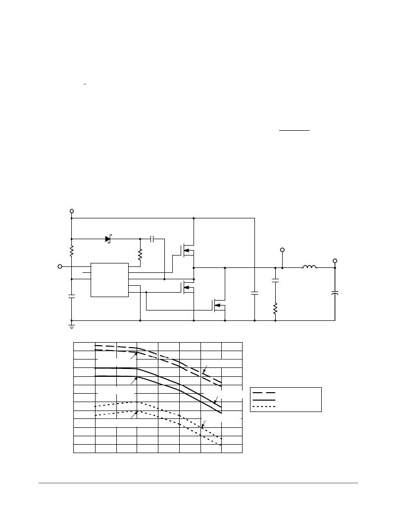
�V� IN� =� 12� V�
�D� BST�
�(Optional)�
�C� BST�
�1.0� m�
�C� O�
�C� VS�
�1.0� m�
�R� VS�
�2.2�
�4�
�5�
�6�
�CO� BST�
�EN� TG�
�V� S� DRN�
�PGND�
�U1� BG�
�NCP5355�
�3�
�2�
�1�
�8�
�7�
�R� GU�
�2.2�
�Q� top�
�NTD60N03�
�Q� bottom1�
�NTD80N02�
�Q� bottom2�
�NTD80N02�
�Switch� Node�
�C� SN�
�4700� p�
�C� IN�
�4.7� m�
�R� SN�
�2.2�
�L� OUT�
�V� CORE� =� 1.40� V�
�+�
�C� OUT�
�Figure� 4.� Typical� NCP5355� Application�
�86�
�85�
�84�
�83�
�82�
�Internal� Diode�
�External� Diode�
�81�
�80�
�79�
�78�
�77�
�Internal� Diode�
�Internal� Diode�
�External� Diode�
�External� Diode�
�200� kHz,� Series� 2�
�400� kHz,� Series� 4�
�600� kHz,� Series� 8�
�76�
�75�
�74�
�73�
�10�
�15�
�20�
�25�
�I� O� (A)�
�Figure� 5.� Efficiency� With� and� Without� an� Added� External� Bootstrap� Diode,� See� Figure� 4� for� Test� Circuit�
�http://onsemi.com�
�7�
�相关PDF资料 |
PDF描述 |
|---|---|
| 1485F60 | WIREWAY 60" STEEL 12X6" GREY |
| VI-BNV-CX-F4 | CONVERTER MOD DC/DC 5.8V 75W |
| T95C107M016LZAL | CAP TANT 100UF 16V 20% 2812 |
| BAV23A-7 | DIODE SWITCH 350MW 200V SOT23-3 |
| GSM06DRKS | CONN EDGECARD 12POS DIP .156 SLD |
相关代理商/技术参数 |
参数描述 |
|---|---|
| NCP5355DR2G | 功能描述:功率驱动器IC 12V 2A Buck Power MOSFET RoHS:否 制造商:Micrel 产品:MOSFET Gate Drivers 类型:Low Cost High or Low Side MOSFET Driver 上升时间: 下降时间: 电源电压-最大:30 V 电源电压-最小:2.75 V 电源电流: 最大功率耗散: 最大工作温度:+ 85 C 安装风格:SMD/SMT 封装 / 箱体:SOIC-8 封装:Tube |
| NCP5355PDR2 | 功能描述:功率驱动器IC 12V 2A Buck Power RoHS:否 制造商:Micrel 产品:MOSFET Gate Drivers 类型:Low Cost High or Low Side MOSFET Driver 上升时间: 下降时间: 电源电压-最大:30 V 电源电压-最小:2.75 V 电源电流: 最大功率耗散: 最大工作温度:+ 85 C 安装风格:SMD/SMT 封装 / 箱体:SOIC-8 封装:Tube |
| NCP5358MNTXG | 功能描述:开关变换器、稳压器与控制器 GATE DRIVERS FOR NOTEBOOK RoHS:否 制造商:Texas Instruments 输出电压:1.2 V to 10 V 输出电流:300 mA 输出功率: 输入电压:3 V to 17 V 开关频率:1 MHz 工作温度范围: 安装风格:SMD/SMT 封装 / 箱体:WSON-8 封装:Reel |
| NCP5359 | 制造商:ONSEMI 制造商全称:ON Semiconductor 功能描述:Gate Driver for Notebook Power Systems |
| NCP5359A | 制造商:ONSEMI 制造商全称:ON Semiconductor 功能描述:Gate Driver for Notebook Power Systems |
发布紧急采购,3分钟左右您将得到回复。