- 您现在的位置:买卖IC网 > Datasheet目录996 > NCP5612GEVB (ON Semiconductor)EVAL BOARD FOR NCP5612G Datasheet资料下载
参数资料
| 型号: | NCP5612GEVB |
| 厂商: | ON Semiconductor |
| 文件页数: | 3/11页 |
| 文件大小: | 0K |
| 描述: | EVAL BOARD FOR NCP5612G |
| 设计资源: | NCP5612 EVB BOM NCP5612GEVB Gerber Files NCP5612 EVB Schematic NCP5612 BOM - V1.0 |
| 标准包装: | 1 |
| 电流 - 输出 / 通道: | 60mA |
| 输出及类型: | 2,非隔离 |
| 输出电压: | 4.8 ~ 5.7 V |
| 特点: | 亮度控制 |
| 输入电压: | 3.6V |
| 已供物品: | 板 |
| 已用 IC / 零件: | NCP5612 |
| 其它名称: | NCP5612GEVBOS |
��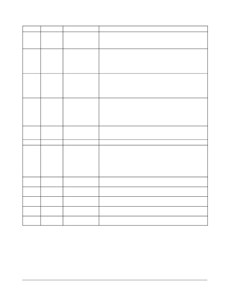 �
�
�NCP5612�
�PIN� FUNCTION� DESCRIPTION�
�Pin� No.�
�1�
�Symbol�
�GND�
�Function�
�POWER�
�Description�
�This� pin� is� the� GROUND� signal� for� the� power� analog� blocks� and� must� be�
�connected� to� the� system� ground.� This� pin� is� the� GROUND� reference� for� the�
�DC/DC� converter� and� the� output� current� control.� The� pin� must� be� connected� to�
�the� system� ground,� a� ground� plane� being� strongly� recommended.�
�2�
�LED1�
�INPUT,� POWER�
�This� pin� sinks� to� ground� and� monitors� the� current� flowing� into� the� first� LED,�
�intended� to� be� used� in� backlight� application.� The� current� is� limited� to� 30� mA�
�maximum� (Note� 2).�
�The� LED1� is� deactivated� when� the� ICON� bit� of� the� LED?REG� register� is� High.�
�The� LED1� is� automatically� disconnected� when� an� open� load� is� sensed� pin� 2�
�during� the� operation.�
�3�
�LED2�
�INPUT,� POWER�
�This� pin� sinks� to� ground� and� monitors� the� current� flowing� into� the� second� LED,�
�intended� to� be� used� in� backlight� application.� The� current� is� limited� to� 30� mA�
�maximum� (Note� 2).� The� LED2� fulfills� the� ICON� function,� LED1� being�
�deactivated,� when� the� ICON� bit� of� the� LED?REG� register� is� High.�
�The� LED2� is� automatically� disconnected� when� an� open� load� is� sensed� pin� 3�
�during� the� operation.�
�4�
�I� REF�
�INPUT,� ANALOG�
�This� pin� provides� the� reference� current,� based� on� the� internal� band?gap�
�voltage� reference,� to� control� the� output� current� flowing� in� the� LED.� A� 1%�
�tolerance,� or� better,� resistor� shall� be� used� to� get� the� highest� accuracy� of� the�
�LED� biases.� An� external� current� source� can� be� used� to� bias� this� pin� to� dim� the�
�light� coming� out� of� the� LED.�
�In� no� case� shall� the� voltage� at� pin� 4� be� forced� either� higher� or� lower� than� the�
�600� mV� provided� by� the� internal� reference.�
�5�
�CNTL�
�INPUT,� DIGITAL�
�This� pin� supports� the� flow� of� data� between� the� external� MCU� and� the�
�NCP5612� internal� registers.� The� protocol� makes� profit� of� a� Single� Wire�
�structure� associated� to� a� Serial� 8� bits� format� data� flow.�
�6�
�7�
�NC�
�V� OUT�
�?�
�OUTPUT,� POWER�
�No� internal� connection�
�This� pin� provides� the� output� voltage� supplied� by� the� DC/DC� converter.� The�
�V� out� pin� must� be� decoupled� to� ground� by� a� 1� m� F� ceramic� capacitor� located� as�
�close� as� possible� to� the� pin.� Cares� must� be� observed� to� minimize� the� parasitic�
�inductance� at� this� pin.� The� circuit� shall� not� operate� without� such� bypass�
�capacitor� connected� across� the� V� out� pin� and� ground.�
�The� output� voltage� is� internally� clamped� to� 5.5� V� maximum� in� the� event� of� no�
�load� situation.� On� the� other� hand,� the� output� current� is� limited� to� 40� mA�
�(typical)� in� the� event� of� a� short� circuit� to� ground.�
�8�
�C2P�
�POWER�
�One� side� of� the� external� charge� pump� capacitor� (C� FLY� )� is� connected� to� this�
�pin,� associated� with� C2N� (Note� 1)�
�9�
�C2N�
�POWER�
�One� side� of� the� external� charge� pump� capacitor� (C� FLY� )� is� connected� to� this�
�pin,� associated� with� C2P� (Note� 1)�
�10�
�C1P�
�POWER�
�One� side� of� the� external� charge� pump� capacitor� (C� FLY� )� is� connected� to� this�
�pin,� associated� with� C1N� (Note� 1)�
�11�
�12�
�V� BAT�
�C1N�
�INPUT,� POWER�
�POWER�
�Input� Battery� voltage� to� supply� the� analog� and� digital� blocks.� The� pin� must� be�
�decoupled� to� ground� by� a� 1.0� m� F� minimum� ceramic� capacitor.�
�One� side� of� the� external� charge� pump� capacitor� (C� FLY� )� is� connected� to� this�
�pin,� associated� with� C1P� (Note� 1)�
�1.� Using� low� ESR� ceramic� capacitor,� 50� m� W� maximum,� is� mandatory� to� optimize� the� Charge� Pump� efficiency.�
�2.� Total� DC/DC� output� current� is� limited� to� 60� mA.�
�http://onsemi.com�
�3�
�相关PDF资料 |
PDF描述 |
|---|---|
| NCV7680PWR22GEVB | BOARD EVALUATION NCV7680 |
| NDNA200 | DIN-RAIL 35MM ALUMINUM 2M |
| NG-9517 | CABLE GLAND NEMA 4X PG-29 BLACK |
| NH2503K000FJ01 | 250WATTS 3KOHMS 1% NON-INDUCTIVE |
| NHN0.50BK | GORILLA SLEEVING 1/2" BLACK 500' |
相关代理商/技术参数 |
参数描述 |
|---|---|
| NCP5612MUTBG | 功能描述:LED照明驱动器 WHITE LED DRIVER- 2LED-SW RoHS:否 制造商:STMicroelectronics 输入电压:11.5 V to 23 V 工作频率: 最大电源电流:1.7 mA 输出电流: 最大工作温度: 安装风格:SMD/SMT 封装 / 箱体:SO-16N |
| NCP561SN15T1 | 功能描述:低压差稳压器 - LDO 1.5V 150mA CMOS RoHS:否 制造商:Texas Instruments 最大输入电压:36 V 输出电压:1.4 V to 20.5 V 回动电压(最大值):307 mV 输出电流:1 A 负载调节:0.3 % 输出端数量: 输出类型:Fixed 最大工作温度:+ 125 C 安装风格:SMD/SMT 封装 / 箱体:VQFN-20 |
| NCP561SN15T1G | 功能描述:低压差稳压器 - LDO 1.5V 150mA CMOS w/Enable RoHS:否 制造商:Texas Instruments 最大输入电压:36 V 输出电压:1.4 V to 20.5 V 回动电压(最大值):307 mV 输出电流:1 A 负载调节:0.3 % 输出端数量: 输出类型:Fixed 最大工作温度:+ 125 C 安装风格:SMD/SMT 封装 / 箱体:VQFN-20 |
| NCP561SN18T1 | 功能描述:低压差稳压器 - LDO 1.8V 150mA CMOS RoHS:否 制造商:Texas Instruments 最大输入电压:36 V 输出电压:1.4 V to 20.5 V 回动电压(最大值):307 mV 输出电流:1 A 负载调节:0.3 % 输出端数量: 输出类型:Fixed 最大工作温度:+ 125 C 安装风格:SMD/SMT 封装 / 箱体:VQFN-20 |
| NCP561SN18T1G | 功能描述:低压差稳压器 - LDO 1.8V 150mA CMOS w/Enable RoHS:否 制造商:Texas Instruments 最大输入电压:36 V 输出电压:1.4 V to 20.5 V 回动电压(最大值):307 mV 输出电流:1 A 负载调节:0.3 % 输出端数量: 输出类型:Fixed 最大工作温度:+ 125 C 安装风格:SMD/SMT 封装 / 箱体:VQFN-20 |
发布紧急采购,3分钟左右您将得到回复。